
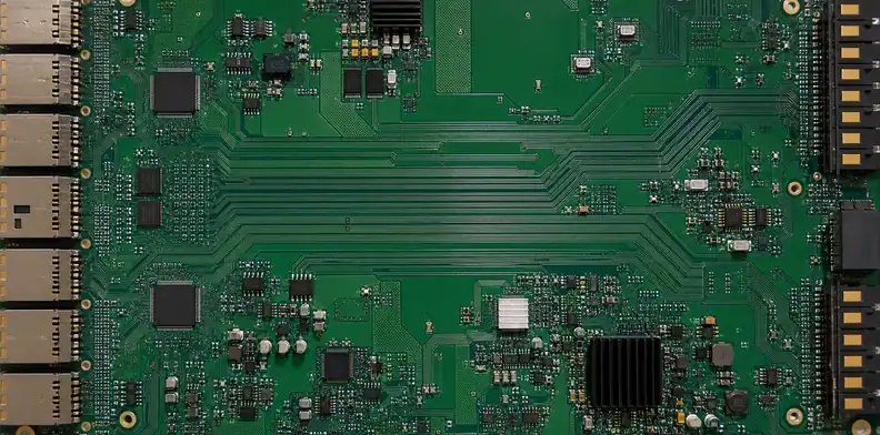
Quick Answer: Large PCB signal integrity depends on electrical length, edge rate, stack-up, reference continuity, loss, crosstalk and interconnects—not board dimensions alone. Identify the longest critical channels, assign continuous reference planes, control impedance with the supplier’s production stack-up, model loss and discontinuities, and define coupon or channel evidence before fabrication.
Large PCB signal integrity becomes a distinct design problem when critical signals travel farther, cross more mechanical zones or pass through connectors at opposite ends of the board. A physically large PCB is not automatically high speed, and a short board is not automatically safe. The governing question is whether propagation delay and discontinuities are significant relative to the signal edge and timing budget.
This article focuses on the large-format delta: long channels, distant return paths, accumulated loss, remote power domains and the manufacturing evidence needed to release an oversized layout.
Table of Contents
- Classify channels by electrical length
- Freeze the stack-up and impedance route
- Keep return paths continuous
- Budget loss across the complete channel
- Control crosstalk over long parallel runs
- Treat vias and connectors as discontinuities
- Coordinate signal and power integrity
- Simulate the cases that can change the layout
- Specify manufacturing and test evidence
Classify channels by electrical length
Treat a trace as a transmission line when its propagation delay is no longer small compared with the driver’s rise or fall time.
Board length is only a proxy. A one-meter industrial control line with slow edges may tolerate routing that would fail a much shorter multi-gigabit link. Conversely, a fast device can create transmission-line behavior even at a modest clock frequency. Use the actual edge rate, signaling standard, dielectric environment and topology.
Create a channel inventory with source, load, data rate, edge rate, maximum routed length, topology, reference plane, connector count and timing or eye-mask requirement. Rank channels by consequence and uncertainty. This prevents the team from applying expensive high-speed rules to every net while missing one long reset, clock or differential pair.
Include asymmetrical routes and asynchronous control signals. A slow clock with a fast output buffer can ring even when its repetition rate appears harmless. Long open-drain or multidrop nets may need termination and pull-up analysis. Record package and connector models when they materially affect the result rather than simulating only the visible PCB trace.
Texas Instruments publishes High-Speed Interface Layout Guidelines that emphasize controlled routing, references and discontinuity management. Apply the device vendor’s current interface guide whenever it is more specific.
Freeze the stack-up and impedance route
Trace width is not an impedance specification until it is tied to a production dielectric stack, copper condition and tolerance.
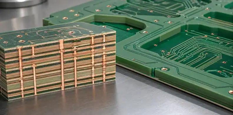
Long traces accumulate the effect of impedance variation. Define the target impedance, tolerance, layer, reference plane and differential geometry. Ask the supplier to return a manufacturable stack-up using the actual laminate family, dielectric thickness and finished copper. Do not copy a calculator width into the drawing and assume the result is controlled.
Identify which nets require controlled impedance and whether coupons represent them. Very long traces may need additional loss characterization beyond a simple impedance coupon. Use the controlled-impedance PCB article for general construction rules and the Large Format PCB manufacturer page for size-route review.
| Channel input | Minimum record | Release evidence |
|---|---|---|
| Signaling standard | Data rate, edge and topology | Vendor limit or simulation target |
| Stack-up | Material, dielectric and copper | Supplier-approved production stack |
| Impedance | Target, tolerance and layer | Coupon plan and test report |
| Length | Routed channel, not board diagonal | Constraint and post-layout extraction |
Do not finalize long critical routes before the supplier-approved construction exists.
Plan impedance tolerance with system margin. A narrower fabrication tolerance can improve consistency but may increase cost or reduce size capability. Model realistic process corners and determine whether the interface truly needs the tighter limit. If it does, make coupon geometry, test frequency and report ownership explicit in the RFQ.
Keep return paths continuous
A signal path is incomplete without a nearby, uninterrupted return path.
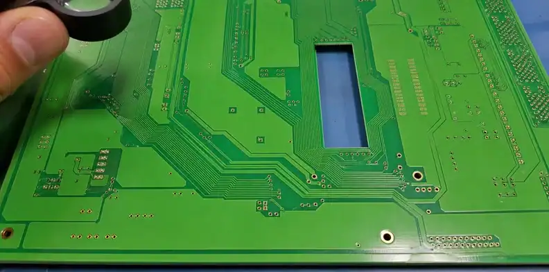
Long boards often contain mechanical slots, isolation zones, split power areas and connector fields. A trace crossing a reference split forces return current to detour, increasing loop area, radiation and susceptibility. Route critical signals over continuous reference planes and keep layer transitions near stitching vias that preserve return continuity.
For differential pairs, field cancellation does not remove the need for a reference. Pair symmetry, spacing and common-mode conversion still depend on the environment. Avoid routing near board edges or long cutouts where the field changes abruptly.
A mechanical revision can invalidate a channel without changing its routed length. When a new slot cuts the reference plane beneath a differential pair, review the copper beneath the entire route, including both launches. Reroute over continuous ground where possible. At a signal-layer transition, confirm that the reference planes are connected by an intentional return path; a nearby signal via alone does not provide one. Save the affected channel extraction with the mechanical revision before accepting the change. TI SPRAAR7J, Section 2.4 explains the return-path effects of reference-plane gaps and ground-plane transitions.
At connectors, provide enough reference pins and a short return path. A signal may be well controlled on both boards yet fail because the connector pin assignment forces return current through a distant ground contact. Review the complete interconnect pinout and cable shield strategy as part of the channel.
Budget loss across the complete channel
Insertion loss must include dielectric and conductor loss plus vias, connectors, launches and any cable transition.
Long copper length increases attenuation and frequency-dependent distortion. Low-loss material can help, but laminate selection should follow a channel budget rather than a generic “high speed” label. Copper roughness, finished copper thickness, solder mask and routing geometry also affect loss.
Build a simple budget early, then refine it with extracted geometry. Include transmitter package or breakout, board routing, vias, connectors and receiver launch. If the interface uses equalization, confirm what loss profile it can tolerate and at which frequencies.
| Loss contributor | Large-board risk | Design response |
|---|---|---|
| Dielectric length | Accumulated attenuation | Shorten route or choose qualified material |
| Copper roughness | Higher high-frequency loss | Use supported foil/material model |
| Vias and stubs | Resonance and reflection | Backdrill or optimize transition when justified |
| Connectors | Launch discontinuity and mode conversion | Use model and controlled footprint |
Use the material-to-signal-speed article for general material comparisons, but validate the final choice in the complete channel.
Do not approve a laminate upgrade unless the modeled channel shows why it is needed.
For a long channel near its loss or timing limit, share the interface standard, routed length, connector model and proposed stack-up in a channel manufacturability review. The review should identify which stack-up and coupon assumptions need supplier approval before layout release.
Keep the electrical budget connected to the physical drawing. Connector location or board-outline changes can add routing length after the original analysis. A post-layout check should compare actual extracted length and transitions with the approved pre-layout case, then record any remaining margin.
Loss is not the only limitation. Dispersion, skew and reflections can close the eye before total attenuation reaches a simple limit. For differential channels, include glass-weave or routing asymmetry where the data rate and length make skew significant. Use phase tuning carefully; added serpentine length can increase loss and local coupling.
Control crosstalk over long parallel runs
Small coupling per unit length can become significant when two routes remain parallel for a long distance.
Increase spacing where long parallelism is unavoidable, keep references close, and route aggressors and sensitive victims on different layers or orientations when practical. Differential-pair spacing rules should preserve pair coupling without creating unnecessary congestion. Avoid a single global clearance that ignores parallel length and edge rate.
Clock, memory, high-current switching and fast control edges deserve special attention. Use field-solver or extraction results for the longest coupled regions. If the board has repeated channels, simulate the worst geometric case and confirm that copied layouts preserve the same reference and spacing.
Guard traces help only when their return connection and spacing are engineered. Adding an unstitched copper line between signals can create another resonant structure rather than a reliable shield.
Treat vias and connectors as discontinuities
Optimize transitions when their discontinuity consumes a meaningful share of the channel budget.
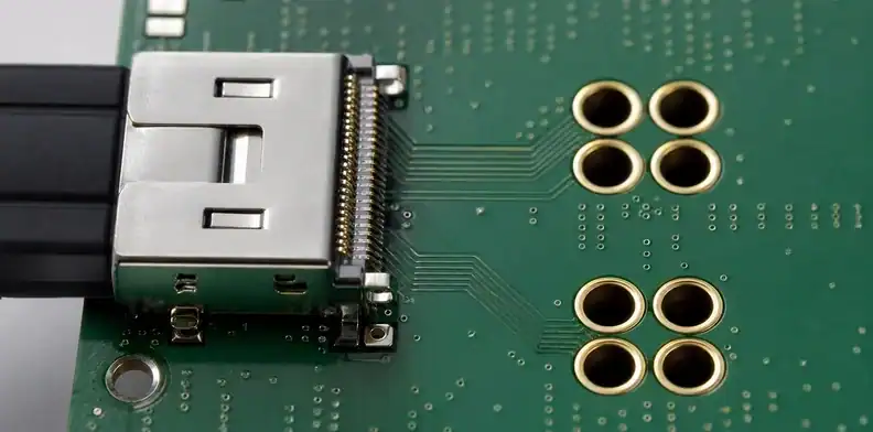
Large boards often use connectors to reach remote modules, while mechanical constraints force layer changes. Each via adds capacitance, inductance and possibly a stub. Connector launches can create impedance steps and differential skew. Minimize unnecessary transitions and keep differential vias symmetric.
Backdrilling, blind vias or specialized connectors can improve performance but add cost and manufacturing risk. Use simulation or measurement to justify them. When a connector dominates the channel, spending heavily on a lower-loss laminate may not solve the actual bottleneck.
Keep reference-via placement, anti-pad geometry and breakout constraints in the fabrication/assembly review. Confirm that tolerances used in the model are manufacturable on the oversized production route.
If test pads or probe points are added, model their stubs on the most sensitive channels. A bring-up feature that helps one team can create a permanent discontinuity for another. Removable probes, short pad structures or dedicated test coupons may provide evidence with less channel impact.
Improve the largest discontinuity first, not the most visually obvious feature.
Coordinate signal and power integrity
Remote devices need a controlled return path and a stable local power network; long power distribution can modulate the same channels being optimized.
Estimate DC drop from source to the farthest load and include connector resistance. Place bulk and high-frequency decoupling according to current path and device guidance. Plane segmentation can solve one power-domain problem while creating a signal-return problem, so review both together.
High-current switching regions should not share narrow return bottlenecks with sensitive receivers. Model or measure power-distribution impedance where transient load and long distance make the margin small. Provide test points that allow bring-up teams to observe remote rails and reference noise.
Thermal and copper-balance decisions can alter plane geometry. Keep SI/PI review connected to DFM so a late copper-thieving or stack-up change does not silently modify critical structures.
Remote clock and data receivers should use local reference quality, not assume the source ground is identical across the board. Estimate ground shift and common-mode range under worst load. When chassis or shield connections exist at multiple points, review return-current paths and EMC together with signal integrity.
Simulate the cases that can change the layout
Model early enough that the result can change topology, layer assignment, connector choice or material.
Pre-layout simulation should compare plausible stack-ups, route lengths and transitions. Post-layout extraction should use actual geometry and include the longest, most discontinuous and most tightly coupled channels. Run meaningful process corners rather than an arbitrary set of perfect nominal cases.
For serial links, inspect insertion/return loss and time-domain or eye results against the interface requirement. For clocks and single-ended control, review reflection, ringing, overshoot, settling and crosstalk. Preserve assumptions with the result so manufacturing substitutions can be checked later.
The eye-diagram article explains how to connect measurement to timing and noise margin.
A screenshot without stack-up, models, corners and pass criterion is not release evidence.
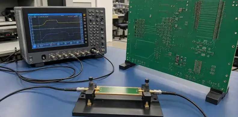
Specify manufacturing and test evidence
The RFQ should identify controlled structures, approved stack-up, coupon design, test quantity, report format and allowed substitutions.
Send impedance requirements by layer and net class. Confirm the coupon represents production geometry and follows the same panel process. State whether impedance results are lot-level, panel-level or serialized. If insertion-loss testing is required, define the method, frequency range and acceptance criterion before quotation.
Review the PCB impedance test report requirements and link every test result to part number, revision, lot and stack-up. A pass result from a different construction is not evidence for the released board.
Define change triggers. A laminate substitution, dielectric adjustment, copper change, alternate connector or modified antipad can invalidate a model even when the schematic and routed length are unchanged. The supplier disposition should separate changes allowed within the approved impedance model from changes that require SI review.
During bring-up, measure representative near-end and far-end points with a setup whose probes and fixtures do not dominate the result. Correlate unexpected ringing or eye closure with the extracted channel before changing termination or equalization. Preserve the working measurement configuration for repeat builds.
Create a channel signoff table and mark unresolved assumptions before fabrication:
| Signoff field | Required entry | Approval owner |
|---|---|---|
| Physical definition | Stack-up revision and routed channel length | PCB design + fabricator |
| Model baseline | Package, connector, via and material models | Signal-integrity engineer |
| Analysis result | Process corners and pass criterion | Interface owner |
| Production proof | Coupon/test method and lot linkage | Quality + supplier |
This makes an engineering waiver visible instead of burying it inside a simulation folder.
For repeated products, correlate coupon results and system performance over lots. Coupon impedance does not prove every discontinuity, but stable coupon data helps distinguish a manufacturing shift from a connector, assembly or firmware issue. Keep the correlation tied to the exact stack-up and route.
FAQ
Does a larger PCB automatically have worse signal integrity?
No. Risk depends on electrical length, edge rate, topology, references and discontinuities. Larger outlines simply make long channels and separated functions more likely.
What is the maximum safe trace length?
There is no universal length. Use driver edge rate, propagation delay, signaling standard, loss budget and topology to decide when transmission-line analysis is required.
Do all long traces need controlled impedance?
No. Apply controlled impedance where interface behavior and edge rate require it. Slow or noncritical nets may need only noise, timing and voltage-drop checks.
Should I choose low-loss laminate for every large PCB?
Only when the channel budget shows ordinary material cannot meet loss or timing requirements with practical routing and transitions.
How should the supplier prove impedance?
Use an approved production stack-up, representative coupon, defined test method and a report tied to the manufactured lot.
Written by the QueenEMS Engineering Team.
Share your longest channels, interface standards and proposed stack-up for a route and evidence review.
Review My Large PCB Signal Path
Upload your files today · Free DFM check before production · Ship worldwide
Get your PCB prototypes in as fast as 24 hours. We handle FR4, Rogers, and hybrid boards up to 40 layers in volume production, with advanced builds subject to engineering review — free prototypes for 2–4 layer FR-4 boards, no minimum order.
Just upload your Gerber + BOM — we source every part, assemble, and inspect (AOI + X‑Ray) so you don't have to chase suppliers. Boards ship in as fast as 24 hours.