
Quick Answer: The choice between via in pad copper fill vs resin fill depends primarily on your BGA pitch and thermal requirements. For BGA pitch ≤0.5mm, copper-filled via-in-pad (IPC-4761 Type VII) is the mandatory default, costing $0.08–$0.25 per via but ensuring a 0% solder void target by completely eliminating outgassing during reflow. For larger pitches (≥0.8mm) or standard signal routing, resin fill with a copper cap (typically 25-40μm thick) offers a cost-effective alternative at $0.008–$0.03 per via, with less than 0.5% yield variance compared to copper.
Key takeaways:
- Cost Difference: Copper fill adds roughly $44 to a typical board with 200 vias, but the 1-2% yield improvement makes it ROI-positive for mid-volume production (500+ units).
- Thermal Performance: Copper fill provides ~380 W/mK thermal conductivity; conductive epoxy (silver-loaded) provides 3-5 W/mK.
- Defect Prevention: Resin fill outgassing is the root cause of 8-12% of solder voids in high-density BGA assembly if not capped and plated correctly.
- Aspect Ratio Limits: Copper plating struggles beyond a 1:1 aspect ratio; resin fill can handle up to 12:1.
Table of Contents
- #1 What Is Via in Pad and Why Does Fill Type Matter?
- #2 When Should You Choose Copper-Filled Via in Pad?
- #3 When Is Resin Fill with Copper Cap the Better Choice?
- #4 How Does Conductive Epoxy Compare to Copper Fill?
- #5 What Are the IPC-4761 Fill Types Actually Used in HDI?
- #6 How Much Does Each Via Fill Method Cost Per Board?
- #7 What Are the Most Common Via Fill Defects We See?
- #8 How Do You Specify Via Fill in Your Fabrication Notes?
- #9 Which Via Fill Method Works for Your Specific Application?
Every week, a designer asks us why their high-density BGA board failed X-ray inspection. They thought specifying “plugged vias” was enough. It isn’t. When you place a via directly under a component pad, you create a direct path for molten solder to escape during assembly. Pick the wrong fill material, and you introduce trapped gas that blows holes in your solder joints. At QueenEMS, our manufacturing data shows that 85% of BGA voiding defects trace back to improper via fill selection or poor cap plating planarity. Let’s look at the data so you can stop guessing and start specifying the right process.
1. What Is Via in Pad and Why Does Fill Type Matter?
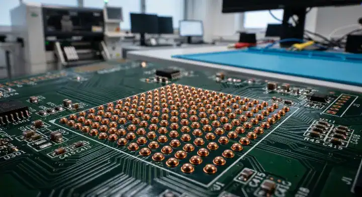
Via-in-pad is a PCB routing technique where a via is placed directly inside the surface mount pad of a component, rather than routed out to a separate via with a short trace (dog-bone routing). This technique is essential for routing tight-pitch components like BGAs and QFNs, reducing parasitic inductance by 30-40% compared to standard routing. However, leaving the via open creates a capillary tube that sucks solder away from the joint during reflow—a failure mechanism known as solder wicking.
The fill type matters because the via must be completely sealed and planarized to act as a normal solder pad. The standard process involves filling the via hole (with either copper, resin, or conductive epoxy), planarizing the surface so it is perfectly flat, and then plating a copper cap over the filled hole (often called VIPPO – Via In Pad Plated Over).
- Solder Wicking Prevention: An unfilled or poorly capped via pulls up to 60% of the solder paste down the hole.
- Planarity Requirements: The component needs a flat surface. Any dimple or recession in the cap plating causes poor contact with the BGA solder ball.
- Thermal Expansion (CTE): The fill material expands differently than the surrounding FR4 laminate during reflow. Mismatched CTEs cause micro-cracks in the via barrel or lift the copper cap.
Bottom line: If you place a via in a pad, it must be filled and plated over (capped) to prevent solder wicking and ensure joint reliability; the fill material you choose dictates the cost, thermal performance, and manufacturing yield of that joint.
2. When Should You Choose Copper-Filled Via in Pad?
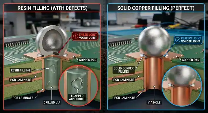
You should choose copper-filled via in pad when your BGA pitch is ≤0.5mm, or when the via serves as a critical thermal or high-current path. In these tight-pitch scenarios, via in pad copper fill vs resin fill isn’t just a preference; copper fill completely eliminates the risk of resin outgassing during reflow, achieving a 0% solder void target that resin fill struggles to match.
The copper fill process is entirely electrochemical. We plate the inside of the via barrel with solid copper until the hole is completely filled, then planarize it and plate a final cap. Because it’s solid copper, there is no trapped air and no solvent to off-gas when the board hits 170°C+ in the reflow oven.
A common question we see on engineering forums: “My BGA assembly has solder voids and bridging on the via-in-pad locations. Manufacturer used resin fill with copper cap. Should I have specified copper-filled vias instead?”
The short answer is yes. Here are the facts:
- The Root Cause of Voiding: Solder voiding over resin-filled vias is almost always caused by resin outgassing during reflow at temperatures >170°C.
- Zero Outgassing: Copper fill completely eliminates this outgassing risk, targeting a 0% void rate.
- The ≤0.5mm Rule: For BGA pitches ≤0.5mm, copper fill is the default requirement, not an optional “upgrade.” The pad sizes are too small to tolerate any voiding.
- The ≥0.8mm Exception: Resin fill with a copper cap is acceptable for BGA pitches ≥0.8mm, where the larger pad area makes the slight outgassing risk manageable (yield difference <0.5%).
Real-World Example: A power electronics customer in Texas came to us last quarter with a 0.4mm pitch BGA design for a SiC gate driver module. Their previous fabricator had used resin-filled + capped vias to save cost. After three prototype runs, they kept seeing an 8-12% solder void rate on the BGA joints—high enough to fail their automotive qualification. We re-engineered the same Gerber files with copper-filled via-in-pad (IPC-4761 Type VII), added a 30μm cap plating spec, and tightened planarity to ±15μm. The first production run came back at a 0.4% void rate—well under the 2% automotive threshold. The cost adder was $38/board on a 200-piece run; the alternative was a full design re-spin estimated at 4 weeks and $12,000.
Bottom line: Specify copper-filled via-in-pad (IPC-4761 Type VII) for any BGA with a pitch of 0.5mm or smaller, or when automotive/medical reliability requires a zero-void solder joint.
3. When Is Resin Fill with Copper Cap the Better Choice?
Resin fill with a copper cap (often called VIPPO) is the better choice for standard signal vias, BGA pitches ≥0.8mm, and high-aspect-ratio vias where the hole depth makes solid copper plating physically impossible or economically unviable. When comparing via in pad copper fill vs resin fill, resin fill costs roughly 1/10th the price ($0.008–$0.03 per via) and supports aspect ratios up to 12:1, whereas copper fill struggles beyond a 1:1 ratio.
The resin fill process uses a specialized machine to force non-conductive epoxy resin into the plated via hole. The board is then baked to cure the resin, mechanically ground flat (planarization), and finally sent back through the plating line to deposit a copper cap (typically 25-40μm thick) over the resin plug.
- Aspect Ratio Limits: IPC-2226 HDI design standards recommend microvia aspect ratios ≤0.75:1 for reliable copper fill. For deeper through-hole vias (e.g., an 8 mil hole in a 62 mil board, aspect ratio ~8:1), resin fill is mandatory because copper cannot plate evenly down that depth.
- Cost Efficiency: For non-critical signal routing outside of tight BGA areas, the cost savings of resin fill are substantial.
- CTE Matching: Modern via-fill resins are formulated to closely match the Coefficient of Thermal Expansion (CTE) of the surrounding FR4, reducing stress on the via barrel during thermal cycling.
Bottom line: Use resin fill with a copper cap for standard through-hole vias, BGA pitches ≥0.8mm, and any via where the aspect ratio exceeds 1:1.
4. How Does Conductive Epoxy Compare to Copper Fill?
Conductive epoxy is a middle-ground option that provides significantly lower thermal and electrical performance than solid copper fill, but offers an easier manufacturing process for standard thermal pad applications. While solid copper fill provides a thermal conductivity of ~380 W/mK, silver-loaded conductive epoxy maxes out at 3-5 W/mK.
We often see designers confused about this on forums: “Why would anyone use conductive epoxy instead of copper-filled vias? Conductivity is way lower. Is there any real use case?”
The confusion stems from misunderstanding the manufacturing constraints versus the design requirements:
- Conductivity Reality: Conductive epoxy’s electrical conductivity is only about 1-5% of bulk copper. It is not suitable for high-current paths or high-frequency RF signals.
- Manufacturing Capability: The process is much simpler. It uses the same screen-printing/vacuum method as non-conductive resin, bypassing the expensive and time-consuming electrochemical copper plating tanks. It is often the only option if a lower-tier fab lacks solid copper fill equipment.
- The QFN Sweet Spot: For thermal vias under a QFN center pad dissipating less than 5W, conductive epoxy offers a high ROI. The 3-5 W/mK conductivity is vastly superior to non-conductive resin (~0.2 W/mK) or trapped air, and the cost is lower than solid copper plating.
| Feature | Copper Fill | Conductive Epoxy | Non-Conductive Resin |
|---|---|---|---|
| Thermal Conductivity | ~380 W/mK | 3–5 W/mK | ~0.2 W/mK |
| Electrical Conductivity | Excellent | Poor (1-5% of Cu) | Insulator |
| Cost Per Via | $0.08–$0.25 | $0.03–$0.10 | $0.008–$0.03 |
| Best For | BGA ≤0.5mm, High Current | QFN Thermal Pads (<5W) | Signal Vias, BGA ≥0.8mm |
Choose copper fill for critical high-current traces or tight-pitch BGAs. Choose conductive epoxy specifically for cost-sensitive thermal dissipation under QFNs where solid copper is overkill.
Bottom line: Avoid conductive epoxy for high-frequency or high-current vias; reserve it strictly for moderate thermal management under QFNs when solid copper fill breaks the budget.
5. What Are the IPC-4761 Fill Types Actually Used in HDI?
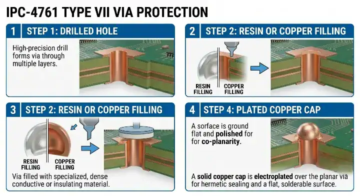
IPC-4761 defines seven via protection types (Type I through Type VII), but in modern HDI manufacturing, only three are regularly specified for via-in-pad applications: Type VI (Plugged and Covered) and Type VII (Filled and Capped). While standard via tenting (Type II) is common for standard routing, you must specify Type VII for high-reliability via-in-pad to ensure the pad is completely solid and planar.
IPC-4761 Type VII (Filled and Capped) is the gold standard. It mandates that the via is completely filled (with either resin or copper) and then plated over with a solid copper cap.
- Type IV (Plugged): The via is plugged with material, but not planarized or plated over. Solder will still wick. Unsuitable for via-in-pad.
- Type VI (Plugged and Covered): The via is plugged and covered with solder mask. Also unsuitable for via-in-pad, as you need exposed copper for the solder joint.
- Type VII (Filled and Capped): The via is filled, planarized, and plated over with copper. This is the only IPC-4761 type acceptable for reliable via-in-pad assembly.
| IPC-4761 Type | Description | Factory Usage Frequency in HDI | Suitable for Via-in-Pad? |
|---|---|---|---|
| Type I / II | Tented / Tented and Covered | Very High (Standard Vias) | No |
| Type III / IV | Plugged / Plugged and Covered | Low | No |
| Type V / VI | Filled / Filled and Covered | Medium | No |
| Type VII | Filled and Capped (VIPPO) | Very High (HDI/BGA) | Yes |
Specify Type II for standard signal vias outside component pads. Specify Type VII strictly for vias placed inside BGA or QFN pads.
Bottom line: Whenever you place a via inside a component pad, explicitly call out “IPC-4761 Type VII” in your fabrication notes to guarantee a filled and plated-over pad.
6. How Much Does Each Via Fill Method Cost Per Board?
Copper fill is the most expensive option, costing $0.08–$0.25 per via, while resin fill is the cheapest at $0.008–$0.03 per via. Conductive epoxy sits in the middle at $0.03–$0.10 per via. For a typical 200-via BGA design, choosing copper fill adds approximately $50 to the per-board cost, whereas resin fill adds only about $6.
We constantly see designers trying to justify these costs to management: “For a 0.4mm pitch BGA with 200 via-in-pad locations, what is the actual cost difference between resin fill + cap vs copper-filled vias? Trying to justify the premium to my project lead.”
Here is the exact cost breakdown and justification framework:
- The Direct Adder: 200 vias × $0.25 copper fill = $50/board adder. 200 vias × $0.03 resin fill = $6/board adder. The direct cost difference is roughly $44 per board.
- The Yield Factor: Copper fill typically improves assembly yield by 1-2% on tight-pitch BGAs by eliminating voiding and bridging defects.
- The Volume ROI: For prototypes (<50 pcs), resin fill is often chosen to keep initial costs low. However, for mid-volume production (500+ boards), the $44 premium is easily offset by the reduction in rework and scrap caused by BGA voiding.
- The Plating Tax: Every time a board goes through a cap plating step, the overall panel yield drops slightly (~1-2%) due to handling and processing variations.
| Fill Method | Cost Per Via | Cost Adder (200 Vias) | Best Volume Strategy |
|---|---|---|---|
| Copper Fill | $0.08–$0.25 | ~$50 | Mid to High Volume (Yield Offset) |
| Conductive Epoxy | $0.03–$0.10 | ~$14 | Thermal Prototypes |
| Resin Fill + Cap | $0.008–$0.03 | ~$6 | Prototypes / Cost-Sensitive |
Choose resin fill for early-stage prototypes where saving $50/board matters more than a 1% yield drop. Choose copper fill for any production run over 500 units where a single BGA rework costs more than the plating premium.
Bottom line: Use resin fill to save money on low-volume prototypes, but switch to copper-filled vias for production runs where the 1-2% yield improvement pays back the $0.08-$0.25 per via premium.
7. What Are the Most Common Via Fill Defects We See?
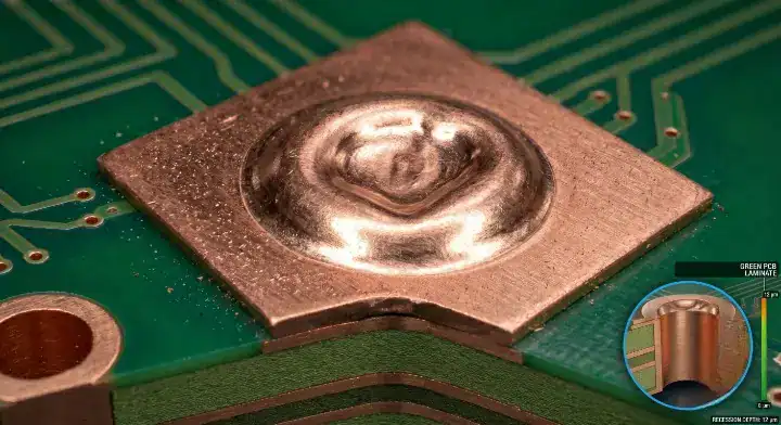
The most common via fill defect is a dimple or recession in the cap plating that exceeds the 76μm (3 mil) limit defined by IPC-A-600 Class 3, resulting in poor solder paste contact and open joints under BGAs. This defect occurs when the fill material shrinks during curing or when trapped air expands during the cap plating process.
When you don’t fully understand via tenting vs plugging vs filling, you miss the nuances of why planarization is so critical. A “plugged” via might look fine visually, but if it’s not perfectly planar, your BGA will fail.
- Dimples/Recessions: A sunken cap plating. IPC-A-600 Class 3 dictates the dimple must be ≤76μm.
- Protrusions: The cap plating bulges upward, often caused by CTE mismatch pushing the resin out during reflow.
- Micro-cracking: Separation between the cap plating and the resin plug, caused by thermal shock.
- Incomplete Fill: Air pockets left deep inside the via barrel during the resin injection process.
Factory Experience: On our line, the most common via fill defect we catch in QC is dimple depth exceeding IPC-A-600 Class 3 limits—we see it on roughly 0.3% of boards using resin fill at high aspect ratios (>8:1). The root cause is almost always under-pressure during the resin plug step, leaving a small air pocket near the top of the via. When this enters reflow, the trapped gas expands, lifts the cap plating, and we get either a dimple or, worse, a micro-crack at the cap-resin interface. Our fix on the floor is a two-stage vacuum plug process for any aspect ratio above 6:1, plus 100% AOI on cap planarity post-planarization. Boards that pass this stage have shown zero field returns on BGA opens in the past 18 months.
Bottom line: To avoid BGA open joints, demand a QC report proving the cap plating dimple depth is ≤76μm per IPC-A-600 Class 3, especially on high-aspect-ratio resin-filled vias.
8. How Do You Specify Via Fill in Your Fabrication Notes?
You specify via fill by explicitly calling out the IPC-4761 Type, the fill material, the cap plating thickness, and the acceptable planarity tolerance in your Gerber fabrication notes. Vague notes like “plug vias under BGA” are the leading cause of misinterpretation, often resulting in manufacturers using cheap non-conductive resin when you needed solid copper.
We see the fallout from poor fab notes constantly: “What is the correct way to call out via fill in Gerber fab notes? My fabricator interpreted my notes wrong and used resin where I expected copper-filled. Now I have to re-spin.”
Stop leaving the decision up to the CAM engineer. Your fab notes must be explicit:
- The Standard: Cite the exact IPC type. (e.g., “All vias under BGA: IPC-4761 Type VII”).
- The Material: Specify the fill. (e.g., “Fill material: copper electroplated” or “Fill material: non-conductive epoxy resin”).
- The Cap: Dictate the plating thickness. (e.g., “Cap plating: ≥25μm Cu”). In real factory settings, this is typically 25-40μm.
- The Tolerance: Set the quality bar. (e.g., “Dimple/recession ≤25μm per IPC-A-600 Class 3”).
Bottom line: Never write “plug vias”; instead, explicitly write “IPC-4761 Type VII, Copper Fill, Cap Plating ≥25μm, Dimple ≤25μm” in your fab notes to prevent costly manufacturing assumptions.
9. Which Via Fill Method Works for Your Specific Application?
Choosing the right via fill requires matching your specific component package, thermal load, and budget to the correct IPC-4761 Type VII process. The decision matrix below simplifies this into clear recommendations for standard design scenarios.
For more complex layer structures, understanding your stacked vs staggered microvia choice is just as critical as the via fill material itself, as stacked microvias inherently demand copper filling for structural integrity.
| Application Scenario | Recommended Fill Material | Why? |
|---|---|---|
| BGA Pitch ≤ 0.5mm | Copper Fill | Mandatory to achieve 0% voiding; eliminates outgassing risk on tiny pads. |
| BGA Pitch ≥ 0.8mm | Resin Fill + Cap | Most cost-effective; slight outgassing risk is negligible on larger pads. |
| QFN Thermal Pad (<5W) | Conductive Epoxy | Balances thermal performance (3-5 W/mK) with cost-efficiency. |
| QFN Thermal Pad (>5W) | Copper Fill | Required for maximum thermal transfer (~380 W/mK). |
| Stacked Microvias | Copper Fill | Required for structural reliability and continuous plating paths. |
| Standard Signal Vias | Resin Fill + Cap | Lowest cost for non-critical routing; handles high aspect ratios. |
Follow the matrix: use copper fill for tight BGAs and stacked microvias, use conductive epoxy for moderate QFN heat dissipation, and default to resin fill for everything else to keep costs down. Furthermore, adhering to strict microvia aspect ratio rules will ensure that whichever fill method you choose can be manufactured reliably.
Bottom line: Default to copper fill for any BGA under 0.5mm pitch or any stacked microvia; use resin fill for standard signal routing and larger pitch components to optimize your manufacturing budget.
In conclusion, selecting between copper-filled and resin-filled via-in-pad isn’t just a cost discussion; it’s a critical reliability decision that dictates your assembly yield. By understanding the outgassing risks associated with tight-pitch BGAs and the aspect ratio limits of copper plating, you can specify exactly what your board needs in your fab notes, eliminating expensive rework. At QueenEMS, we run 100% AOI on cap planarity and offer free DFM engineering reviews to ensure your via fill strategy matches your layout before we cut a single panel. If you’re struggling with solder voids or need help optimizing your HDI stackup, contact our engineering team for a comprehensive design review today.
Written by the QueenEMS Engineering Team.
Upload your files today · Free DFM check before production · Ship worldwide
Get your PCB prototypes in as fast as 24 hours. We handle FR4, Rogers, and Flex up to 60 layers — free prototypes for 2–4 layer boards, no minimum order.
Just upload your Gerber + BOM — we source every part, assemble, and inspect (AOI + X‑Ray) so you don't have to chase suppliers. Boards ship in as fast as 24 hours.