
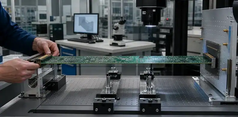
Quick Answer: Control large PCB connector alignment with one functional datum system shared by the PCB, connectors and enclosure. Include fabrication, placement, reflow, board shape and mating-part variation in the tolerance stack. Add deliberate float where permitted, then verify position, angle and mating force on the assembled first article.
Two connectors can each meet their local footprint dimensions and still refuse to mate in the chassis. Across a long board, small position, rotation and shape errors combine with housing cutouts, standoffs and mating-card tolerances. Forcing the interface may bend pins, load solder joints or hold the PCB in a permanent twist.
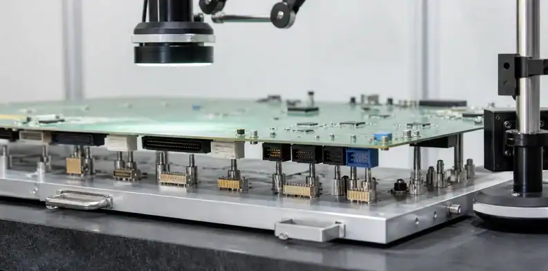
The challenge is to make widely separated connectors mate with each other and with the enclosure without forcing the board into position. Start with the datum planning in large PCB design rules and the drawing practices in hole-position datum control, then check the combined alignment of the complete mating system.
Table of Contents
- Define the functional mating relationship
- Build the complete tolerance stack
- Choose a locating and restraint strategy
- Place connectors from local and global datums
- Account for reflow, board shape and temperature
- Design compliance instead of forced fit
- Measure the first article in assembly state
- Send an alignment-ready RFQ
Define the functional mating relationship
Alignment requirements should describe what must mate and what is allowed to move, not only where pads appear in Gerber data. Begin with the connector manufacturer’s permissible axial, lateral and angular misalignment, then connect those limits to PCB and enclosure datums.
Identify the center of guidance
Multi-connector applications need a deliberate center or sequence of guidance. Samtec recommends establishing a connector center of guidance before calculating multi-connector misalignment. One interface may locate the assembly while another accommodates accumulated variation through float, lead-in or compliant mounting.
Mark the primary connector, guiding pins, mating direction and insertion sequence on the assembly drawing. Without that hierarchy, several nominally precise features can over-constrain the product and fight each other during mating.
Separate electrical contact from mechanical location
Pins and solder joints should not become the default structure that pulls misaligned hardware into position. Use connector alignment features, chassis guides, dowels, bosses or controlled float according to the component design. The electrical interface then operates within its intended misalignment and wipe range.
Record which surfaces or pins locate X, Y and Z, which feature controls rotation and which directions remain free until final seating. This degree-of-freedom model gives mechanical, PCB and assembly teams the same interpretation.
Build the complete tolerance stack
The stack must include every contributor between mating interfaces: PCB feature position, board scale and shape, connector footprint and housing, placement, solder self-alignment or shift, mounting holes, standoffs, sheet-metal/plastic features and the mating assembly.
| Contributor | Evidence source | Typical decision |
|---|---|---|
| PCB pad and hole position | Fabrication drawing and supplier capability | Select datum and inspection method |
| Connector geometry | Manufacturer drawing | Use allowed float, lead-in and mating range |
| Placement and reflow | Assembly capability and first-article measurement | Set local fiducials and program criteria |
| Board bow/twist | Agreed flatness method | Decide support state during measurement/mating |
| Enclosure cutout/boss | Mechanical drawing and inspection data | Allocate position and size tolerance |
| Mating board/cable | Interface control drawing | Include the opposite half, not just this PCB |
Use worst-case analysis where every unit must fit at simultaneous extremes, or an approved statistical method when process distributions and risk justify it. Do not switch between methods silently. The connector’s allowable misalignment is the budget; the stack shows how much each contributor consumes.
Keep X, Y, Z and angular stacks separate until the interface definition combines them. A small rotation around a board datum can create a large linear offset at a distant connector, while a Z-height error may reduce contact wipe even when XY centers align. The analysis should use the same reference plane and sign convention as the drawings.
Allocate tolerance to processes that can actually control and measure it. Tightening the finished outline does not fix pad-to-pad distance, and tightening pad position does not correct a loose chassis boss. For each contributor, record the supplier, measurement method and data available at first article. An unmeasurable allocation is not a useful procurement requirement.
Evidence check: Every tolerance contributor needs a controlling drawing source and feasible measurement method.
Choose a locating and restraint strategy
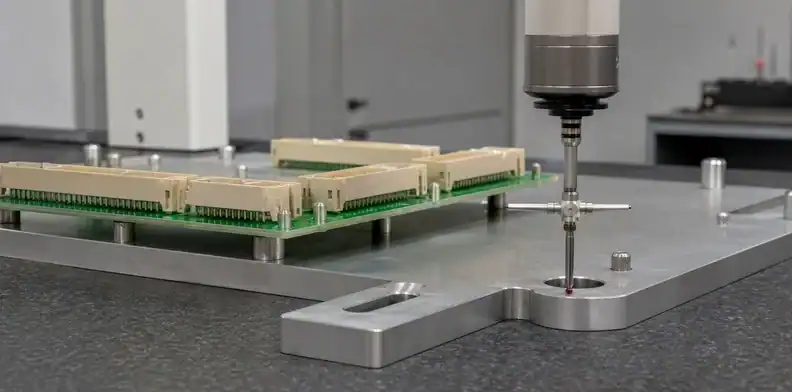
A stable scheme usually constrains the required degrees of freedom once and avoids duplicating the same constraint at distant features. Hole-and-slot mounting is one common method: a round feature locates two axes, a slot controls rotation while allowing expansion or accumulated distance variation.
Use functional datums on the drawing
Set datum A from the installation plane, datum B from the primary locating feature and datum C from the orientation feature, or use an equivalent project-specific scheme. Dimension critical connector and mounting relationships from these datums rather than chaining dimensions across the board.
Add basic dimensions, position tolerances, material condition where appropriate and measurement-state notes with mechanical engineering approval. Fabricators should not infer enclosure function from artwork alone.
Avoid distant hard constraints
Two tight round holes at opposite ends can require the PCB and chassis to match an unrealistic center distance after material and temperature variation. Similarly, multiple rigid board-to-board connectors may each attempt to locate the same axes.
Convert one distant feature to a slot, floating bushing, compliant connector or guided interface when system requirements permit. This is not “making the design loose”; it is placing precision where it controls function and allowing harmless variation elsewhere.
Place connectors from local and global datums
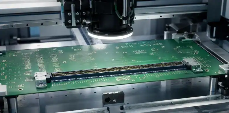
Connector placement needs both a global board reference and local fiducials near fine-pitch or long connector footprints. Global fiducials establish the product coordinate system; local references reduce the effect of board-scale distortion and camera/placement variation near the interface.
Keep CAD data internally consistent
The PCB pads, mechanical holes, connector outline, centroid coordinates and 3D model must come from one released library and revision. Compare the assembly drawing and interface-control drawing against the generated fabrication and placement data. A correct footprint in the wrong coordinate revision still creates a fit failure.
Control centroid rotation conventions, board origin and panel transformation. Ask the assembler to confirm how fiducials are used for each connector and whether placement is single-pass. Long boards should not be reloaded from a different origin without an approved registration strategy.
Review solder self-alignment conservatively
Surface tension can center compatible soldered components within a limited offset, but it does not repair an incorrect datum system or a multi-connector enclosure stack. AMD’s official carrier-card guidance provides one product-specific example of combining PCB pad position and placement tolerance; its numerical limits must not be copied to unrelated connectors.
Use the connector manufacturer’s land pattern, paste design and self-alignment guidance. Measure post-reflow housing position and angle on the first article rather than accepting pre-placement coordinates as final proof.
| Registration stage | Working reference | Evidence retained |
|---|---|---|
| PCB fabrication | Functional datum holes and pads | Dimensional inspection result |
| SMT placement | Global and local fiducials | Program revision and placement check |
| Post-reflow | Connector housing or mating face | Position, angle and coplanarity data |
| Chassis assembly | Interface datums and guides | Functional gauge or mating result |
Placement rule: Final connector location is a post-reflow measurement, not a centroid-file assumption.
Account for reflow, board shape and temperature
The mating relationship can change between room-temperature fabrication, reflow and installed operation. Long spans amplify rotation from small end-to-end position differences, while bow and twist move connector faces out of plane.
Define the support state for connector measurement. A free board, a carrier-supported PCBA and a chassis-fastened assembly may show different positions. The acceptance condition should match the interface being protected; do not flatten the board on a metrology table if it mates unsupported in the product.
Review copper balance and thermal profile where reflow shape affects alignment. Nearby supports should react connector insertion without forcing the laminate. The large PCB stiffener and support article explains the load-path decision once the required connector location is known.
Temperature also changes the relative distance between PCB, metal chassis and polymer housings. Mechanical engineering should evaluate the operating range and material expansion for precision interfaces. Slots, float and flexible interconnect may absorb predictable movement better than tighter fabrication tolerances.
Connector coplanarity deserves its own check where long housings or multiple interfaces share a mating plane. Board twist can leave one end seated and the other lifted, even though center positions appear acceptable from above. Measure the mating face in three dimensions or use a functional gauge that detects tilt without forcing the housing flat.
Shipping and service can alter the relationship after factory acceptance. Heavy cable harnesses, repeated mating and chassis flex apply moments to distant connectors. If those loads are credible product conditions, include local supports and a verification cycle rather than relying on the first static fit.
Design compliance instead of forced fit
Compliance is a controlled capability of the connector or mounting system to accept misalignment without overstressing contacts, solder joints or the PCB. It should be selected from a quantified tolerance stack, not added after a prototype refuses to mate.
Match float to the remaining budget
Floating board-to-board connectors, guided headers, compliant pins, cable assemblies and rigid-flex transitions provide different freedom. Use manufacturer data for allowable X/Y, axial and angular motion, mating force, wipe, cycle life and electrical performance.
Do not count the mating pair as two independent sources of float. In Harwin’s FLECTO C05701 specification, Appendix 2, the floating mechanism is in the male connector; the female has none. The F10 series lists ±0.5 mm movement in each of the X, Y and Z axes during mating and when mated. Those values apply to that series. For the selected connector, compare the accumulated positional error and expected operating movement with the available travel in the manufacturer’s coordinate system.
The required float must exceed the approved residual stack with margin defined by product engineering. Too little float produces force; uncontrolled excess can weaken guidance, shielding or high-speed performance.
Document the allowed motion in the connector coordinate system and verify that harnesses, shields and mounting hardware do not consume it. A floating connector trapped by a stiff cable or tight panel cutout no longer provides the compliance assumed by the tolerance analysis. Include the installed surrounding parts in the first-article exercise.
Control insertion force and support
Measure mating force and provide a local reaction path through chassis supports or stiffeners. A connector at the end of a long unsupported bay can deflect the PCB even when positional alignment is acceptable. That deflection may crack solder joints or make another connector appear misaligned.
For a contextual interface check, send the connector drawings, board/enclosure models, datum scheme and tolerance stack through the QueenEMS DFM review. The useful return is a fabrication/assembly feasibility disposition and a list of dimensions that remain customer-owned system requirements.
Decision point: Assign each constrained degree of freedom once and preserve deliberate compliance elsewhere.
Measure the first article in assembly state
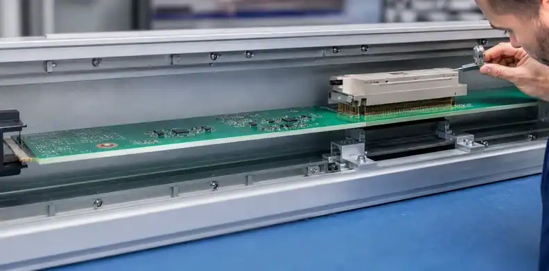
First-article evidence should prove the functional relationship after soldering and with the intended hardware. Measure connector center/angle, mounting features, board shape and mating behavior from the approved datums.
Use a coordinate measurement method, optical system, dedicated gauge or functional mating fixture suited to the tolerances. Record instrument, setup, support state, temperature, board/assembly serial, connector lot, fixture revision and actual results. A “fits” photograph cannot replace dimensional data when the interface has a tight budget.
Compare at least the primary locating connector and the most distant constrained interface in the same setup. Moving the assembly between independent fixtures can introduce a new registration uncertainty that hides the end-to-end relationship. A common gauge, interface-control fixture or coordinated measurement plan keeps both results tied to the functional datum system.
Where the mating half is supplied by another vendor, identify its measured or certified condition rather than treating nominal CAD as truth. Quarantine a mismatch until the two sides are reconciled; otherwise each supplier may report conformance to a different interpretation while the system remains unbuildable.
Preserve the gauge setup and mating-part identity with the report. A future lot cannot be compared credibly when the reference hardware, support state or insertion sequence has changed without a recorded equivalence review.
Perform a controlled mating test without using excessive force to pull parts together. Inspect connector housings, pins, solder joints and board deformation before and after. If a deviation is accepted, document its effect and whether the tolerance model, drawing or process must change before the remaining lot.
Send an alignment-ready RFQ
An RFQ should include the fabrication data and the mechanical interface definition that gives those features meaning. Send Gerber or ODB++, drill files, stack-up, centroid, assembly drawings, 3D board model, connector manufacturer drawings, enclosure/mating-part interfaces, datum scheme, critical position tolerances, support hardware and expected quantities.
Request post-reflow position evidence, board-shape measurement, fixture/gauge plan and any special placement or mating validation. Identify who approves changes to connector footprint, fiducials, mounting slots, tolerance allocation and enclosure features.
Require suppliers to state measurement capability against the allocated tolerance rather than quoting only nominal dimensions. The response should identify whether results come from optical inspection, coordinate measurement, a functional gauge or customer-supplied mating hardware. Where a feature cannot be measured by the proposed method, resolve the evidence plan before the purchase order.
Quotation request: Send the controlled interface package with the QueenEMS large-board quote form. The response should separate proposed fabrication datums, assembly registration, first-article measurements and any open system-level alignment assumptions.
Release rule: Do not use assembly force to disposition an interface that has not passed shared datum criteria.
FAQ
Why do connectors align in CAD but fail in the enclosure?
Because CAD nominal positions do not include fabrication, placement, reflow, board shape, hardware and mating-part variation. The physical interface needs a full tolerance stack and locating scheme.
Should every connector use local fiducials?
Not necessarily. Use local fiducials where connector pitch, length, board scale or placement risk warrants them, and confirm the assembler’s actual vision strategy before release.
Can solder self-alignment correct connector position?
Only within the connector and paste system’s qualified range. It cannot correct a wrong footprint, incompatible datum chain or enclosure mismatch.
Are two tight mounting holes better than a hole and slot?
Not for every long assembly. Two distant tight holes can over-constrain center distance; a properly oriented slot may preserve rotation control while accepting harmless longitudinal variation.
What should stop production after the first article?
Stop when connector position, mating force, board shape or interface fit falls outside the approved criteria, or when the measurement setup cannot trace results to the released datum scheme.
Sources
- Samtec: Tolerance Stack Up in Multi-Connector Applications
- AMD UG1091: PCB Fabrication and Assembly House Requirements
Written by the QueenEMS Engineering Team
Upload your files today · Free DFM check before production · Ship worldwide
Get your PCB prototypes in as fast as 24 hours. We handle FR4, Rogers, and hybrid boards up to 40 layers in volume production, with advanced builds subject to engineering review — free prototypes for 2–4 layer FR-4 boards, no minimum order.
Just upload your Gerber + BOM — we source every part, assemble, and inspect (AOI + X‑Ray) so you don't have to chase suppliers. Boards ship in as fast as 24 hours.