
Quick Answer: A production-ready pcb test point design requires adding dedicated 0.9mm to 1.0mm copper pads for every electrical net, spaced at a 1.27mm minimum center-to-center distance. Providing 100% test access on the bottom side of your board prevents a $4,500 to $10,000 fixture redesign fee during mass production and cuts testing time from 4 minutes down to 30 seconds per board.
Key takeaways:
- Target 100% net coverage to detect 98% of assembly defects.
- Maintain 0.9mm–1.0mm pad diameters for standard in-circuit test (ICT) fixtures.
- Keep a 1.27mm center-to-center spacing to prevent pogo pin physical collisions.
- Consolidate 100% of test points to the bottom side to avoid costly dual-side fixtures.
Table of Contents
- Why Do Test Points Matter for PCB Assembly and Production?
- What Are the Minimum Test Point Size and Spacing Rules for ICT?
- Where Should You Place Test Points on Your PCB Layout?
- How Many Test Points Do You Need for Adequate Test Coverage?
- What Is the Difference Between Test Point Requirements for ICT vs Flying Probe?
- How Do Test Points Affect PCB Layout Density and Routing?
- What Happens When You Design a Board Without Adequate Test Access?
- Test Point Design Checklist for Production-Ready PCBs
- FAQ
Getting a printed circuit board manufactured is only the beginning; verifying that it functions correctly dictates your project’s success. Many hardware engineers ignore pcb test point design during the initial layout phase, viewing it as an afterthought rather than a core requirement. QueenEMS maintains a 99.7% first pass yield rate specifically because we require our clients to integrate strict electrical testability before moving to mass production. If you wait until the pilot run to consider how the factory will test your board, you face expensive fixture delays or painfully slow manual testing protocols.
Why Do Test Points Matter for PCB Assembly and Production?
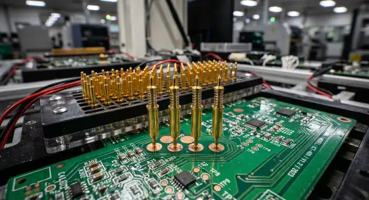
A test point is a dedicated, exposed copper pad on a PCB used to make direct electrical contact during manufacturing verification via automated pogo pins. When a layout includes 100% net coverage through these dedicated points, factories can run automated tests that detect up to 98% of assembly defects like shorts, opens, and missing components in under 30 seconds per board.
Here is the reality: Factories rely on physical access to verify soldering quality and component functionality. Without designated pads, automated equipment cannot inject signals or measure resistance across the assembled board.
Test points serve three specific purposes throughout a product’s lifecycle:
- Development characterization: Engineers probe these pads manually with oscilloscopes during initial prototype bring-up.
- Manufacturing verification: Automated ICT fixtures press hundreds of pogo pins against these pads simultaneously to verify assembly accuracy.
- Field troubleshooting: Technicians use these known locations to diagnose failures in returned units without guessing which trace carries which signal.
A solid PCB design for test DFT strategy builds these access locations into the schematic from day one, preventing production roadblocks.
Bottom line: Failing to add test points forces your manufacturer to test boards manually or skip electrical verification entirely, heavily increasing the risk of shipping dead-on-arrival products to your customers.
What Are the Minimum Test Point Size and Spacing Rules for ICT?
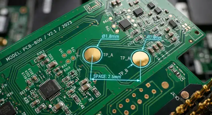
For reliable ICT bed-of-nails probing, the minimum test point size is a 0.9mm to 1.0mm diameter pad, accompanied by a minimum center-to-center spacing of 1.27mm (50 mils) between adjacent points. These hard limits exist because the physical pogo pins inside the test fixture require specific mechanical clearances to operate without bending or shorting against each other.
Many engineers ask on hardware forums exactly how large these pads must be. If you make the pad too small (under 0.8mm), the pogo pin contact becomes unstable, causing false failure readings. If you place them too close together, the fixture manufacturer physically cannot drill the support plate closely enough to mount the spring-loaded pins.
Follow these exact sizing rules based on standard IPC guidelines (IPC-7351 and IPC-D-356):
- Target pad diameter: 1.0mm (39 mils)
- Absolute minimum pad diameter: 0.9mm (35 mils)
- Target center-to-center spacing: 2.54mm (100 mils)
- Absolute minimum center-to-center spacing: 1.27mm (50 mils)
- Clearance from component bodies: 3.0mm (118 mils) minimum
Think about it this way: The physical springs and barrels of the pogo pins dictate your layout rules. You cannot cheat physics when designing the fixture interface.
Bottom line: Always default to 1.0mm pads with 1.27mm spacing for ICT; anything smaller guarantees mechanical clearance failures inside the test jig.
Where Should You Place Test Points on Your PCB Layout?
Place 100% of your test points on the bottom side of the PCB to avoid the $10,000+ cost of a dual-side ICT fixture, while keeping all pads at least 2mm away from board edges to allow room for the fixture’s vacuum seal or mechanical clamps.
Scattering access pads across both the top and bottom layers is a common layout mistake. A single-sided fixture only requires wiring and probes on one half of the clamshell, cutting tooling costs in half.
| Placement Location | Recommended Status | Reason / Impact |
|---|---|---|
| Bottom side (solder side) | Highly Recommended | Requires only a single-sided fixture, saving $5,000+ in tooling costs. |
| Top side (component side) | Avoid | Forces a dual-sided fixture build, doubling costs and complicating maintenance. |
| Within 2mm of board edge | Avoid | Interferes with mechanical clamps and vacuum seals used to hold the board. |
| Underneath components | Forbidden | Physically impossible for a probe to reach the pad without crushing the part. |
| Distributed evenly across board | Highly Recommended | Prevents board warping when hundreds of spring-loaded pins apply upward pressure. |
Choose bottom-side placement if you want to keep fixture costs under $5,000; choose dual-side placement only if your board is extremely dense and bottom-only access is physically impossible.
What does this mean for you? You must consciously route signals to the bottom layer specifically for testing purposes.
- Group test pads in accessible areas rather than hiding them between tall components.
- Maintain a 3mm physical clearance from tall parts like electrolytic capacitors.
- Distribute the points evenly so the 8-ounce spring force per pin does not snap the PCB in half when the fixture engages.
Bottom line: Force all your test access points to the bottom layer of the board; this single layout decision directly halves your mass production testing budget.
How Many Test Points Do You Need for Adequate Test Coverage?
Adequate test coverage requires exactly one accessible test point per electrical net, achieving a 100% net coverage target that allows the test equipment to detect every single short, open, or misplaced component.
A client recently asked us to review a 6-layer motor controller board with 280 components. Their initial layout had 120 test points scattered randomly, with 40% located on the top side near tall electrolytic capacitors. This configuration was physically impossible for a standard bed-of-nails fixture. We consolidated all points to the bottom side, moved 15 points that were too close to the board edges, and increased 22 undersized pads from 0.7mm to 1.0mm. The resulting fixture achieved 98% net coverage, cost $11,000 to build, and processed each board in 22 seconds. If we had tried to build a fixture around their original layout, it would have required a dual-side mechanism costing roughly $22,000—double the cost for the exact same coverage.
| Coverage Level | Typical Test Point Density | PCB Area Impact | Cost Impact |
|---|---|---|---|
| 100% Net Coverage | 1 TP per net | High (Requires dedicated routing) | $10K fixture, $0.15 per board test cost |
| 80% Net Coverage | Missing access on minor nets | Medium | Misses 20% of defects, high field failure risk |
| 50% Net Coverage | Power and major buses only | Low | Requires functional testing backup, slow throughput |
| 0% (No Test Points) | 0 TPs | None | Forced to use $4/board flying probe or manual testing |
Target 100% coverage if you are building medical, automotive, or industrial devices where field failures are unacceptable; accept 80% coverage only if physical space absolutely prohibits full access on low-cost consumer gadgets.
The truth is: You do not need a point on every single component pin, just one point somewhere on the continuous electrical net connecting those pins.
- Start by placing points on all power and ground rails.
- Add points to all programming interfaces and communication buses (SPI, I2C, UART).
- Add points to all analog signal paths and high-value passive networks.
Bottom line: Do not stop routing until your CAD software confirms every single net has at least one dedicated, accessible 1.0mm pad on the bottom layer.
What Is the Difference Between Test Point Requirements for ICT vs Flying Probe?
ICT requires minimum 0.9mm pads and 1.27mm spacing because physical pogo pins must fit inside a custom-drilled fixture plate, whereas flying probe testers can target much smaller 0.6mm pads with 0.6mm spacing because independent robotic arms position the probes individually without physical housing constraints.
Equipment from companies like Keysight Technologies dictates strict fixture parameters for volume manufacturing. While ICT needs a custom bed-of-nails, a flying probe machine uses software-controlled arms to move 4 to 8 probes across the board, making it highly flexible but much slower.
| Parameter | ICT Requirement | Flying Probe Requirement |
|---|---|---|
| Minimum Pad Size | 0.9mm – 1.0mm | 0.6mm (Can probe some component pads directly) |
| Minimum Spacing | 1.27mm (Center-to-center) | 0.6mm |
| Tooling Cost (NRE) | High ($5,000 – $15,000+) | Zero (Software programming only) |
| Test Time Per Board | Fast (15 – 30 seconds) | Slow (2 – 10 minutes) |
Use flying probe if you are running prototypes (5–50 units) where paying $10,000 for a fixture makes no financial sense; use ICT if you are running mass production (1,000+ units) where spending 4 minutes per board on a flying probe creates a massive factory bottleneck.
We see this timing bottleneck frequently. A client with a 1,000-unit industrial sensor run requested our 24-hour fastest turnaround service. Because their dense layout completely lacked ICT access, we were forced to run the batch through our flying probe machines. Testing took 3 days instead of 1 day due to the 4-minute per-board cycle time. For their next revision, they added proper 1.0mm test pads, allowing us to build an ICT fixture that cut test time by 85%.
Let’s break this down: * Flying probe is best for low-volume, high-mix production.
- ICT is mandatory for high-volume, low-mix production.
- Designing for ICT automatically makes the board compatible with flying probe, but designing only for flying probe makes the board impossible to test via ICT.
Bottom line: Always design your PCB using the stricter ICT rules (1.0mm size, 1.27mm spacing), which guarantees compatibility with any testing method the factory chooses to use.
How Do Test Points Affect PCB Layout Density and Routing?

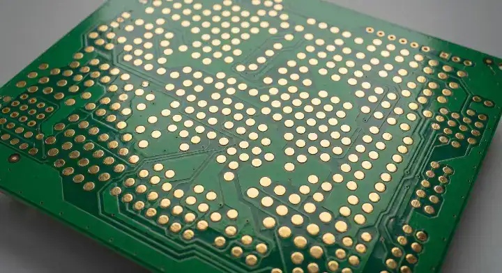
Adding dedicated 1.0mm test pads to every net consumes 3–5% of the total board area and heavily restricts trace routing channels, often forcing engineers to use untented vias as test targets to save space on high-density interconnect (HDI) boards.
When you cannot fit a dedicated 1.0mm circular pad, converting an existing via into a test point is an acceptable alternative. However, the via must remain untented—meaning the solder mask layer must be pulled back to expose the copper ring.
| Via Type | Can Be Used As TP? | Requirements / Limitations |
|---|---|---|
| Standard Through-Hole Via | Yes | Must be untented. Annular ring must be >0.9mm. |
| Tented Via | No | Solder mask physically blocks electrical contact. |
| Microvia / Blind Via | No | Too small (usually <0.4mm); pogo pins will slip or damage the via. |
| Via-in-Pad | Depends | Only if the pad itself meets the 0.9mm size requirement. |
Choose untented standard vias as test targets if you are struggling with board density and need to hit 100% coverage; avoid using any microvias as targets because the mechanical force of the pogo pin will crack the delicate barrel structure.
The good news? Modern CAD tools automate much of this checking.
- You can set up Design Rule Checks (DRC) to verify that all test points sit on the bottom layer.
- You can automatically flag any test point covered by solder mask.
- When evaluating AOI vs X-ray vs ICT, remember that visual inspection cannot verify under-component routing, making physical test access even more critical.
Bottom line: If you lack space for dedicated pads, use standard through-hole vias as your test targets, but strictly verify that the solder mask is removed from those specific vias in your Gerber files.
What Happens When You Design a Board Without Adequate Test Access?
Designing a board without adequate test access forces you to choose between a $4,500 PCB redesign with a 3-week delay, or paying for slow flying probe testing that adds $3.50 per board to your ongoing mass production costs.
Engineers on Reddit frequently complain about getting a frantic call from their contract manufacturer right as pilot production starts. A recent client sent us a 4-layer IoT board with 160 SMT components for a 2,000-unit production order, expecting standard ICT verification. When our engineering team analyzed the Gerber files, only 62% of the nets had accessible test points. The engineer had not added dedicated pads, and almost all vias were tented with solder mask. Building a fixture with only 62% access would miss massive numbers of potential defects. The client faced a brutal choice: redesign the PCB to add the missing points (costing $4,500 and 3 weeks) or use flying probe testing instead. While flying probe works technically, the test time jumped from 25 seconds to 4 minutes per board. This added $3.50 per board, resulting in $7,000 in testing costs for just the first run. They chose to halt production and redesign. Two hours of layout work upfront would have prevented this entire disaster.
It gets worse: * If you skip testing entirely, defective units reach the field, destroying your brand reputation.
- If you rely solely on manual multimeter testing, your labor costs will eliminate your profit margin.
- If you lack test access during functional testing EVT DVT PVT, your firmware engineers cannot easily debug hardware faults.
Bottom line: Failing to plan your test access during layout directly translates into thousands of dollars in lost tooling fees, slower production, and delayed time-to-market.
Test Point Design Checklist for Production-Ready PCBs
A production-ready PCB test point design must pass a 5-point verification: 100% net coverage, bottom-side placement, 1.0mm minimum pad size, 1.27mm center-to-center spacing, and untented vias if used as test targets.
Before you lock your layout and send your files to a manufacturer for DFM PCB design review, run through these exact parameters. Do not assume your layout software will catch these issues automatically unless you specifically configure your constraints.
Keep this in mind:
- Verify your netlist report shows 100% coverage.
- Check the solder mask layer in a Gerber viewer to confirm all test pads are exposed copper.
- Measure the distance from the board edge to the nearest test point to guarantee a 2mm clearance.
Bottom line: Treat test points exactly like high-priority electronic components; if they are missing from the layout, the board is not finished and should not be sent to fabrication.
Frequently Asked Questions (FAQ)
Can I use a 0.5mm pad as a test point for ICT? No, a 0.5mm pad is too small for standard ICT pogo pins. The physical spring-loaded pins require a minimum 0.9mm diameter to make reliable contact without slipping and causing false failures. If you must use smaller pads, you will be forced to use flying probe testing. Contact your factory before using undersized pads.
What is the minimum spacing between two test points? The absolute minimum spacing is 1.27mm (50 mils) center-to-center for standard ICT. The physical housing barrels of the pogo pins inside the fixture will collide if placed any closer together. To prevent fixture redesigns, configure your CAD software to enforce this 1.27mm clearance rule automatically.
Do I need a test point on every single pin of a microcontroller? No, you only need one test point per electrical net, not per physical pin. As long as the testing machine can inject a signal into the continuous copper trace connecting those pins, it can verify the entire net. Route your single point to an open area on the bottom layer to save space.
Can I use normal vias as test points to save space? Yes, but only if the vias are untented. The solder mask must be pulled back to expose the copper ring, and the annular ring must be large enough (ideally 0.9mm) to support the pogo pin. Check your Gerber solder mask layers carefully before submitting your files to manufacturing.
Will flying probe testing work if my board has no dedicated test points? Yes, but it adds severe time and cost penalties. A flying probe machine can target component solder joints directly, but testing takes 2 to 10 minutes per board compared to 30 seconds for ICT. This makes it financially unviable for high-volume manufacturing. Design your boards with ICT access to keep your mass production options open.
Getting your layout right the first time eliminates the stress of factory delays and fixture redesigns. The cost of adding test points in CAD is zero; the cost of fixing a board without them easily exceeds $10,000.
QueenEMS provides a free DFM and DFT engineering review on every single order, catching missing test access before you pay for tooling. We handle everything from prototype flying probe runs to mass-production ICT setups with a 99.7% first-pass yield.
Ready to manufacture your verified design without the hidden fixture fees? Contact QueenEMS for full turnkey PCB assembly and let our engineering team review your test coverage today.
Written by the QueenEMS Engineering Team
Upload your files today · Free DFM check before production · Ship worldwide
Get your PCB prototypes in as fast as 24 hours. We handle FR4, Rogers, and Flex up to 60 layers — free prototypes for 2–4 layer boards, no minimum order.
Just upload your Gerber + BOM — we source every part, assemble, and inspect (AOI + X‑Ray) so you don't have to chase suppliers. Boards ship in as fast as 24 hours.