
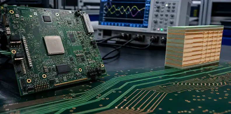
Quick Answer: PCB glass weave skew is a differential-pair timing error caused by the two traces seeing different local dielectric environments, even when their routed lengths match. Treat it as a stack-up and routing-release issue when the channel timing budget is tight: identify the glass style, signal-layer construction, routing angle, and supplier’s actual material option before layout is frozen. A length-match report alone cannot prove that the pair will see the same effective dielectric constant.
- Glass weave skew is different from ordinary trace-length mismatch.
- The fabric style, resin distribution, routing angle, and pair geometry all influence the risk.
- A supplier should confirm the proposed stack-up rather than silently substitute a nominally similar prepreg.
- A useful release package names the critical interfaces and asks how the finished construction will be controlled.
PCB glass weave skew can consume timing margin after a design has already passed a conventional length-matching review. The reason is physical: woven glass bundles and resin do not behave as one electrically uniform material. One member of a differential pair can spend more of its route over glass-rich areas while the other sees more resin-rich areas. The pair may be geometrically symmetric in CAD but electrically asymmetric on the finished board.
This is not a reason to specify exotic laminate on every digital board. It is a reason to decide early whether the interface, layer construction, and channel budget make material-induced skew worth controlling. The laminate selection overview is the starting point for comparing material families; this article addresses the narrower question of what must be checked when woven reinforcement becomes part of the timing problem.
Table of Contents
- What makes glass weave skew different from length mismatch
- Which stack-up details set the risk
- When should a high-speed pair be treated as critical
- How routing can reduce exposure without hiding it
- What the fabricator must confirm before release
- How to use coupons, models, and samples
- What to put in the RFQ and release record
What makes glass weave skew different from length mismatch
Glass weave skew is the timing difference created when two nominally matched conductors travel through different local mixtures of fiberglass and resin. Fiberglass and resin have different dielectric behavior, so the effective dielectric constant below one trace need not match the effective dielectric constant below the other. The resulting delay difference can appear even when the CAD tool reports zero length mismatch.
This differs from a routing mistake. A length mismatch is visible from artwork and can be corrected by changing the trace path. Weave-induced skew depends on the finished dielectric construction, the alignment of the artwork with the panel, and the local relationship between each trace and the glass bundles. Its magnitude is not a universal number for a named laminate because glass style, resin content, dielectric height, and trace geometry also matter.
The practical consequence is that a design review needs two questions. First, is the pair length-matched within the interface budget? Second, could the specified layer construction create a material difference large enough to consume the remaining budget? The second question belongs in the stack-up conversation, not only in the layout review.
Siemens’ fiber-weave analysis describes the effect as a source of differential timing issues in high-speed PCB design. That is useful context, but it does not create a universal routing rule. The board owner must decide from the channel budget whether this effect is material to the product.
Decision point: Treat glass weave as a controlled design input when an interface has little differential-skew margin after package, connector, via, and trace effects are accounted for.
Which stack-up details set the risk
The material family name is not enough to assess this risk. Ask for the actual signal-layer construction: the core or prepreg designation, glass style, nominal pressed dielectric thickness, copper foil type, and whether the fabricator can propose an equivalent construction. A phrase such as “low-loss FR-4” does not identify the local glass and resin geometry seen by the pair.
Glass style matters because the bundle pitch and distribution affect the chance that the two traces see unlike dielectric regions. Resin content matters because it changes the proportion of resin between and around those bundles after lamination. A thin dielectric can make the conductor more sensitive to the material directly beneath it, while a different trace width or pair spacing changes the field distribution. None of these inputs should be assumed from a generic layer-count table.
| Stack-up input | Why it matters to skew | What to request |
|---|---|---|
| Glass style | Sets bundle geometry and local uniformity | Named fabric style or supplier construction code |
| Pressed dielectric | Changes conductor-to-dielectric field coupling | Finished thickness after lamination |
| Resin content | Changes glass-rich and resin-rich distribution | Core/prepreg data and press-out assumption |
| Trace geometry | Changes how much field samples each region | Finished copper, width, spacing, and mask state |
| Artwork orientation | Alters how pairs cross the weave pattern | Routing-angle or panel-orientation note |
For a material-selection review, compare this information alongside the high-speed hybrid stack-up evidence already requested for loss and impedance. The same stack-up cannot be judged as electrically controlled if critical signal layers are left as open supplier substitutions.
Material check: Ask for the exact glass construction before a timing-sensitive pair is treated as production-ready.
When should a high-speed pair be treated as critical
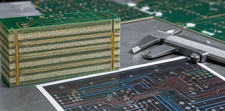
Not every differential pair needs a weave-specific requirement. Start with interfaces whose timing budget is already tight because of data rate, pair length, package escape, connector discontinuities, or accumulated channel loss. A short local connection with generous timing margin may only need ordinary impedance and length control. A long pair crossing a large board, a backplane path, or a dense BGA escape should receive a separate review when the design cannot absorb unexplained skew.
The owner of the interface should define the accepted evidence. That may be a field-solver model using the approved construction, a supplier stack-up with glass style stated, a test coupon strategy, or a prototype measurement plan. Do not ask a fabricator to guarantee an arbitrary skew value without giving the pair class, layer, length range, and measurement boundary. A promise without a test definition produces a dispute, not a controlled build.
An internal pair class makes the handoff clearer. For example, classify pairs as ordinary, timing-sensitive, and channel-critical. The class can then govern whether a release requires only impedance notes, a named glass style, or a measured prototype correlation. This is more useful than placing the same warning on every net.
The controlled-impedance PCB design and manufacturing article can help define the impedance portion of that handoff. It does not replace the extra material information needed for skew-sensitive pairs.
How routing can reduce exposure without hiding it
Routing can reduce the probability that one conductor follows a consistently glass-rich path while the other follows a resin-rich path. Depending on the layout and stack-up, designers may use an angle to the weave, spread-glass construction, a layer change, or a different pair arrangement. The correct choice depends on the interface and manufacturing constraints; it is not a license to add arbitrary serpentine routing.
Do not trade one problem for another. Extra length, abrupt bends, unnecessary via transitions, and poor reference-plane continuity can damage a channel more predictably than the weave effect being addressed. A routing modification should be modeled or justified against the real timing and impedance objective. When the layout cannot move because of BGA pin escape or connector geometry, specify the material control instead of pretending that artwork angle solved the entire issue.
The release drawing should make the critical layer obvious. A short note can identify the differential-pair class, signal layers, approved stack-up revision, and whether alternative glass styles require engineering approval. This lets CAM identify an unintended construction change before fabrication begins.
For dense escape regions, the HDI construction overview provides the broader context for microvia, build-up, and routing-density decisions. Keep the weave decision separate: it is about the dielectric environment around a time-sensitive pair.
Routing call: Change the route only when the revised path is preferable within the channel budget, not merely because it crosses the weave differently.
What the fabricator must confirm before release
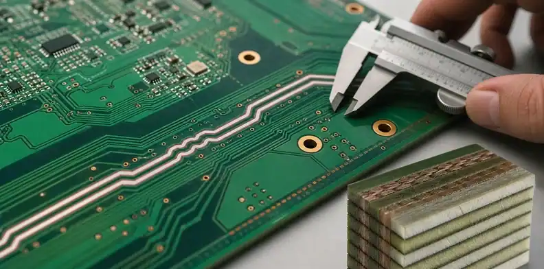
The fabricator should confirm the construction that will actually be pressed, not merely acknowledge the material family in the Gerber notes. A useful response identifies the proposed core and prepreg, glass style or construction code, expected pressed thickness, finished copper, and any change from the design stack-up. If the supplier cannot provide those fields, the buyer cannot tell whether two quotes describe the same electrical board.
This matters most when an approved material is unavailable. An equivalent laminate can still use a different reinforcement style or resin system. The supplier may be able to maintain nominal impedance by changing trace width, yet the substitution can change skew behavior or loss. Require a written proposal that states the affected layers and the intended electrical comparison before the design owner approves it.
A compact release question is more effective than a vague instruction: “For the timing-sensitive pairs on L3 and L14, state the proposed dielectric construction, pressed thickness, glass style, and any artwork-orientation constraint. Do not substitute the named construction without written approval.” This gives CAM a direct escalation path.
When an alternate construction is proposed, use the supplier stack-up sign-off process to keep the accepted table tied to one revision. The approval record should carry the same stack-up revision shown on the fabrication drawing.
How to use coupons, models, and samples
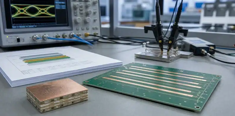
Coupon and prototype work should answer a defined question. A conventional impedance coupon can show whether a controlled line is near its target, but it may not by itself prove worst-case differential skew across all artwork orientations. A model can explore sensitivity to glass style and routing angle, while a prototype can reveal whether the chosen construction behaves acceptably in the actual fabrication and assembly flow.
For a new platform, choose a few representative pair geometries rather than trying to measure every route. Include the longest or most timing-sensitive pair, the escape pattern that forces the tightest geometry, and any layer whose construction differs from the rest of the channel. Preserve the board orientation and material revision in the test record. Otherwise a later repeat order cannot be compared with the original result.
The buyer should define what happens after the result. A successful sample may release the construction for the named revision. A result near the margin may trigger a spread-glass option, route adjustment, or supplier-controlled stack-up change. A failed sample should not be resolved by quietly changing both material and routing, because the root cause becomes impossible to trace.
For a production test package, pair this evidence with PCB impedance test report requirements. Ask the supplier to state what the report represents and which board construction it came from.
| Pair class | Evidence needed | Release response |
|---|---|---|
| Ordinary | Standard impedance stack-up | No special weave note |
| Timing-sensitive | Named glass construction and layer | Engineering review of alternatives |
| Channel-critical | Construction, model or measurement plan | Freeze material and routing revision |
Evidence check: A length-match report is incomplete evidence when the pair’s dielectric environment remains unspecified.
What to put in the RFQ and release record
Use a two-stage request. At quotation, ask whether the supplier can build the named signal layers with the desired glass construction and what controlled alternatives exist. At release, replace that exploratory request with the exact approved stack-up and a change-control instruction. Separating the stages prevents a preliminary availability answer from becoming an accidental production specification.
The RFQ should tell a supplier whether glass weave is a normal material detail or a release-sensitive channel constraint. Send the controlled-impedance stack-up, the relevant net or layer class, material callouts, a note on approved substitutions, and the evidence expected before production. Do not bury the requirement in a generic electrical note where it can be separated from the affected layers.
For an early quote, it is enough to ask whether the supplier can support the named construction and what alternatives they would offer. Before release, freeze the actual stack-up. The approved record should list the material construction, pressed dielectric values, finished copper values, and the owner who accepts an alternative. That record is more valuable on a repeat order than a paragraph claiming that the board is “high speed.”
A release note should also state the decision owner. The fabricator can validate its proposed construction; the electrical owner must decide whether a change remains inside the channel budget. Naming that boundary avoids the common failure where a purchasing substitution is treated as an engineering approval simply because no one answered a generic quote question.
QueenEMS can review a timing-sensitive stack-up when you provide the layer table, critical interface list, pair layers and geometry, intended data rate, and any timing budget already allocated to the PCB. The result can be a quote-ready construction review and a list of supplier questions before a material change reaches production. Use the QueenEMS contact page to submit that package.
FAQ
Can length-matched pairs still have glass weave skew?
Yes. Equal CAD length does not ensure equal effective dielectric conditions. The risk comes from the local material environment around each conductor, so a timing-sensitive design needs both length control and a defined stack-up.
Does every high-speed PCB need spread glass?
No. Spread glass is a material option, not a universal default. Use it when the interface timing budget, route length, and construction sensitivity justify the added control.
Can a supplier change glass style if impedance remains in tolerance?
Not without approval for a skew-sensitive layer. Nominal impedance can remain acceptable while the dielectric construction relevant to differential timing changes. The supplier should identify the proposed substitute and the affected layers.
What is the first file to send for a weave-skew review?
Send the stack-up table. Add the critical layers, pair geometry, interface timing requirement, and any drawing note that limits substitutions. Gerbers alone rarely reveal the material acceptance boundary.
Sources
- Siemens, Preventing glass-weave skew
- IPC, Base Material Consideration for High Speed Printed Circuit Boards
Written by the QueenEMS Engineering Team
Upload your files today · Free DFM check before production · Ship worldwide
Get your PCB prototypes in as fast as 24 hours. We handle FR4, Rogers, and hybrid boards up to 40 layers in volume production, with advanced builds subject to engineering review — free prototypes for 2–4 layer FR-4 boards, no minimum order.
Just upload your Gerber + BOM — we source every part, assemble, and inspect (AOI + X‑Ray) so you don't have to chase suppliers. Boards ship in as fast as 24 hours.