
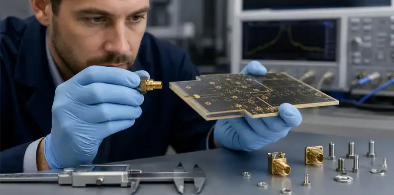
Quick Answer: RF edge launch PCB thickness must match the chosen connector’s mechanical interface and the stackup used to create the launch impedance. Before ordering, lock the connector part number, finished board thickness and tolerance, local edge profile, copper and mask condition, reference-plane geometry, and the inspection method; otherwise a board can meet its overall thickness note yet still fit or perform poorly at the launch.
Key takeaways
- Connector selection, RF launch geometry, and PCB fabrication notes are one release decision.
- A model-specific thickness range is not permission to use any value inside that range without checking the launch design.
- Board edge, copper pullback or edge plating, solder mask, routing quality, and connector seating can affect repeatability.
- A first-lot fit check should use the actual connector hardware and the released PCB revision before a production quantity is approved.
RF engineers often choose an end-launch or edge-launch connector because its center conductor can meet a microstrip or coplanar waveguide near the board edge. The transition looks simple in a footprint, but the physical interface depends on the final board, not the CAD outline alone.
The purchase question behind RF edge launch PCB thickness is therefore broader than “Can you make a 1.6 mm board?” The buyer needs to know whether the finished stackup fits the connector, whether the launch geometry still produces the intended impedance, and whether routing, plating, mask, and assembly will hold the same relationship across the lot.
This article covers fabrication and release evidence for a hybrid RF board. It does not replace connector-vendor simulation or a full electromagnetic launch design. It shows what the PCB/PCBA RFQ must preserve after engineering selects the connector.
Table of Contents
- Lock the connector before freezing the stackup
- Define local thickness at the launch interface
- Control the routed edge and exposed copper
- Keep RF geometry tied to the final build
- Separate fabrication checks from connector assembly
- Approve first-lot fit and electrical evidence
- Send a quote-ready edge-launch package
Lock the connector before freezing the stackup
Select the exact manufacturer part number and termination style before the PCB thickness is released. Soldered edge launches, clamp-style parts, and solderless compression mounts do not share one mechanical envelope. Even connectors with the same coax interface can use different slots, launch-pin heights, mounting holes, torque, or footprint geometry.
Use the current connector drawing as the authority. Record its revision or download date in the design package, especially when a distributor model and the manufacturer’s latest drawing differ. The footprint, 3D model, drill pattern, board thickness range, edge position, and recommended launch should all refer to the same part.
Samtec’s public precision RF material, for example, lists some solderless edge-launch series for boards from about 1.02 mm to 2.54 mm and shows a launch pin around 0.18 mm on the illustrated construction. Those figures are connector-family examples, not universal PCB limits. A different series or soldered part may need a different board interface.
| Connector decision | File to control | RFQ risk when missing |
|---|---|---|
| Exact part number | Approved AVL/BOM line | Footprint matches a different variant |
| Termination style | Connector drawing | Assembly method and edge profile conflict |
| Board interface | Stackup and mechanical drawing | Finished board does not seat correctly |
| Launch reference design | RF layout note or vendor model | Impedance tuning uses the wrong geometry |
Selection rule: Freeze the connector and its current drawing before treating board thickness or launch artwork as production data.
Define local thickness at the launch interface
The fabricator needs a finished board thickness and an allowed range from an authoritative design or connector requirement. That dimension should refer to the finished PCB at the connector location, including the material construction and any feature that changes the clamped or soldered interface.
A nominal 1.60 mm board may be acceptable for one connector and unusable for another. A thin 0.762 mm RF test board may produce the intended microstrip geometry but leave a clamp designed for a thicker board unable to seat. Adding an improvised shim after fabrication can change mechanical reference, ground contact, assembly repeatability, and the validated RF transition.
Do not confuse overall board tolerance with local dielectric thickness. The transmission line is controlled by trace geometry, copper, the distance to the reference plane, dielectric properties, and nearby solder mask or ground features. The connector body may react to total thickness while the RF impedance reacts to a local part of the stackup.
Use PCB board thickness selection for the broader mechanical and cost decision. The hybrid stackup drawing should then identify which layers form the RF launch and which layers only provide structural or digital functions.
Thickness signal: Approve a nominal thickness only after the connector fit and the RF transmission-line geometry both use that same finished construction.
Control the routed edge and exposed copper
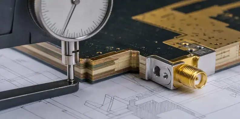
An edge-launch transition ends at a fabricated edge, so routing quality and copper treatment can become electrical and mechanical inputs. The drawing should show the board-edge datum, connector centerline, launch-pad relationship, mounting holes, any notch or step, and whether copper is allowed to reach the edge.
Automatic CAM checks may pull copper away from a routed outline. That is normally protective, but it can conflict with a launch that intentionally brings top ground or edge plating to the profile. Analog Devices notes in its RF launch discussion that poor edge routing can leave an unwanted gap, and it recommends putting required edge plating in the fabrication notes when that feature is part of the RF structure.
If edge plating is required, define the plated segment, connected layers, copper artwork, clearance, surface finish, and acceptance view. Do not write “plate all edges” when only the connector zone needs it. If exposed copper rather than metallized edge is intended, state the mask opening and confirm that routing will not tear or smear the conductor.
| Edge feature | Drawing must state | Evidence to request |
|---|---|---|
| Standard routed edge | Datum and profile tolerance | Dimensional report or first-piece check |
| Copper to the edge | Exact segment and layer | Edge photo and continuity where applicable |
| Metallized edge | Plated length, connected copper, finish | Visual/cross-section plan agreed for the lot |
| Local notch or step | Width, depth, radius, and datum | Measured first-lot dimensions |
Connect this decision to PCB copper-to-edge clearance requirements so intentional launch copper is separated from unintended clearance violations elsewhere on the board.
Edge rule: Treat the launch edge as a controlled RF feature; generic profile notes are not enough when copper or plating is part of the transition.
Keep RF geometry tied to the final build
The launch should be reviewed against the fabricator’s proposed dielectric thickness, copper weight, plating, material data, etch compensation, solder mask, and reference-plane location. If CAM changes a trace width or dielectric thickness to meet impedance, the connector transition may also need review because the taper and ground spacing were tuned with the original geometry.
Ask engineering to identify the frequency range and the performance evidence needed. Some commercial applications only require a controlled impedance transition and functional test. Higher-frequency test, radar, or microwave products may justify a connector-vendor reference design, simulation, time-domain measurement, or vector network analyzer data on a representative launch. The method should follow the product, not a copied marketing claim.
The high-frequency hybrid PCB stackup RFQ article covers material placement and references. This page adds the mechanical endpoint: the final edge and connector must remain consistent with those electrical assumptions.
A useful approval package shows the as-designed launch beside the fabricator’s processed geometry. Highlight trace width, gaps, mask opening, ground-via placement, edge location, and the relevant dielectric. Small changes may be acceptable, but they should not be invisible.
Geometry check: Reopen RF approval whenever CAM changes the trace, gap, reference plane, mask, plating, or edge relationship used by the connector launch.
Separate fabrication checks from connector assembly
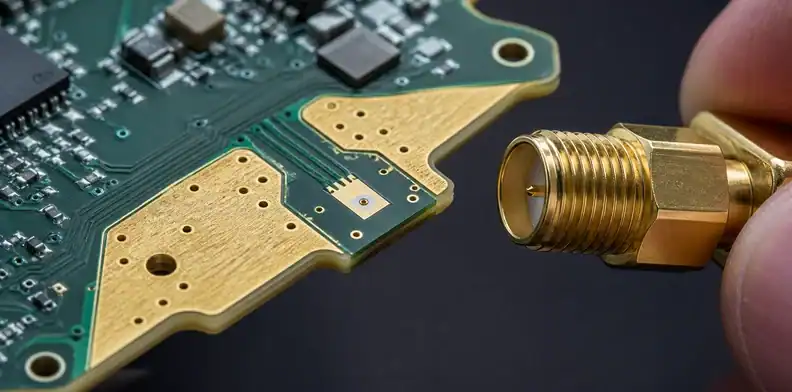
PCB conformance and connector installation are related but different. The fabricator controls stackup, thickness, routing, copper, finish, mask, drill, and inspection. The assembler controls board handling, connector seating, soldering or compression, screw hardware, torque when specified, cleaning, and visual or electrical verification.
Write the work instructions so neither supplier assumes the other owns the missing step. If bare boards ship to a separate EMS, include the connector drawing, assembly notes, hardware, and any keepout or grounding requirements in the PCBA package. The receiving inspection for the PCB should confirm the dimensions and surface condition before connectors are installed.
For a compression mount, seating and hardware can affect repeatability. For a soldered launch, coplanarity, solder flow, heat input, and ground attachment matter. Do not use a solder fillet to compensate for a connector that does not fit the board thickness. The mechanical interface should be correct before the soldering process begins.
The assembly drawing should also define whether the connector is removable for test, whether a fixture supports alignment, and whether the launch is inspected before enclosure installation. These details affect labor and test access, so they belong in the quote.
Ownership call: Put PCB dimensions in the fabrication drawing and installation controls in the assembly drawing, then reference both from the RFQ.
Approve first-lot fit and electrical evidence
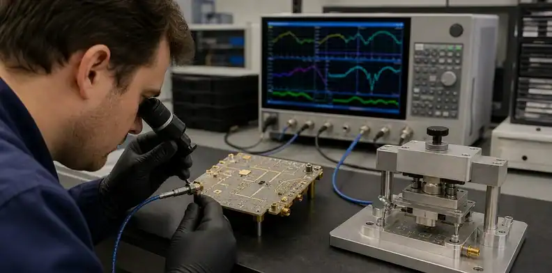
The first lot should prove the interface with the actual connector variant. A dimensional report can confirm finished thickness and edge features. A fit check confirms seating, mounting-hole alignment, launch-pin position, and ground contact. Electrical evidence confirms whether the complete connector-to-board transition meets the agreed need.
Do not approve production from a bare-board photograph alone. A board can look clean but leave a gap under the connector, misplace the center pin relative to the pad, or create a launch discontinuity. Conversely, one good RF measurement without dimensional records may be difficult to reproduce on the next lot.
| First-lot item | Owner | Release question |
|---|---|---|
| Finished thickness and edge dimensions | PCB fabricator/quality | Does the board match the controlled mechanical interface? |
| Connector seating and hardware | PCBA/engineering | Can the part be installed without forcing or shimming? |
| Visual or X-ray evidence where relevant | Quality | Are ground and center-conductor joints acceptable? |
| RF measurement or functional result | RF engineering | Does the assembled transition meet the agreed performance need? |
Tie measurement files to the connector part number, PCB revision, stackup revision, board serial or lot, fixture, calibration approach, and pass criterion. That record makes a later change review much faster.
Use first article inspection for PCB versus AOI to separate conformance evidence from routine optical inspection.
Release point: Approve volume only after one controlled record connects PCB dimensions, connector fit, assembly condition, and the required electrical result.
Send a quote-ready edge-launch package
For PCB fabrication, send Gerber or ODB++ data, stackup, material callouts, finished thickness, edge profile, drill/rout files, impedance notes, copper and mask instructions, edge-plating details, quantity, and inspection requirements. Include the connector drawing and a marked launch image even when the fabricator is not assembling the connector.
For PCBA, add the BOM with exact connector part number, assembly drawing, installation hardware, solder or compression instructions, inspection method, cleaning requirement, fixture information, and electrical test definition. State whether connectors are consigned, supplier-sourced, or approved from an alternate channel.
Ask the supplier to list every assumption: selected stackup, achievable thickness range, edge-routing method, copper treatment, finish, CAM tuning, connector assembly scope, and first-lot evidence. Any proposed thickness or launch change should return to RF engineering before the quote becomes a PO.
A practical note can read: “Quote the PCB and connector interface to the attached revisions. Confirm finished thickness at the edge launch, routed profile, copper and mask condition, edge plating where shown, processed RF geometry, connector seating method, and first-lot fit/electrical evidence. Hold before changing the connector, stackup, launch geometry, or board-edge feature.”
That package gives both the PCB factory and the assembler the same physical reference, which is the simplest way to prevent a late fit dispute.
FAQ
Can I choose any PCB thickness inside the connector’s listed range?
No. A published range only describes part of the mechanical capability for that connector family. The selected thickness must also work with the exact launch geometry, reference plane, hardware, assembly method, and performance target.
Is edge plating always required for an RF edge launch?
No. It depends on the connector, frequency, transition design, grounding approach, and validated reference geometry. When it is required, show the exact segment and connected copper in the fabrication notes.
Should the PCB fabricator install the RF connector?
Not necessarily. A separate PCBA supplier may install it. The RFQ must state ownership and provide the same connector drawing, board revision, assembly controls, and evidence requirements to both parties.
What should I measure on the first lot?
Measure the controlled board thickness and edge geometry, confirm connector seating and hardware alignment, inspect the center and ground connections, and run the electrical or functional verification defined by RF engineering.
Send QueenEMS your PCB and edge-launch requirements
If your PCB or PCBA project uses an RF edge-launch connector on a Rogers, PTFE, FR4, or hybrid stackup, send QueenEMS the connector part number, current drawing, fabrication data, stackup, board-edge details, quantities, and test requirement through the contact page. We can review the fit and fabrication boundary, close open DFM questions, and quote the bare-board and assembly scope with first-lot evidence defined.
Sources
Written by the QueenEMS Engineering Team
Upload your files today · Free DFM check before production · Ship worldwide
Get your PCB prototypes in as fast as 24 hours. We handle FR4, Rogers, and Flex up to 60 layers — free prototypes for 2–4 layer boards, no minimum order.
Just upload your Gerber + BOM — we source every part, assemble, and inspect (AOI + X‑Ray) so you don't have to chase suppliers. Boards ship in as fast as 24 hours.