QUOTE NOW

Rigid 4-layer bare boards · Factory in Shenzhen, China

4-Layer PCB Manufacturing

QueenEMS is a 4 layer PCB manufacturer with 10+ years in PCB manufacturing. Send your files for a review and quote.

A 4-layer Gerber set can leave the construction open. Confirm the layer order, thickness and impedance requirements before fabrication.

Stackup still open? Start with Compare layer plans in the buyer tasks below.

Request a review and quote

Only email is required.

Up to 50 MB: ZIP, RAR or Gerber/drill files. Put PDF drawings, ODB++ data or several files into one ZIP or RAR. The file uploads as soon as you select it.

2 h

Bare PCB quotes are typically sent within 2 hours of receiving complete Gerber files.

5 days

Standard 4-layer lead time under 1 m²; expedited builds from 24 hours.

±5%

Standard impedance tolerance; TDR test report supplied with controlled-impedance orders.

100%

Electrical test (flying probe or fixture) and AOI on every board.

Before you send files

Close these three gaps before ordering

Each gap below is a common fab-note omission, with the detail that closes it.

A layer count and thickness leave the construction open

Two boards can both be 4 layers and 1.6 mm thick and still have very different insulating gaps between the outer copper layer L1 and the inner layer L2. That gap helps determine the trace width needed for a given impedance. Finished thickness and its tolerance also need to suit the connectors.

On a fab note: ‘FR-4, 4L, 1.6 mm, 1 oz’ leaves the core and prepreg construction unspecified.

Board ABoard B
Same total thickness, different L1–L2 gap. Illustration, not to scale.

Check: state the finished thickness with its tolerance, the inner and outer copper weights, and whether your drawing fixes the insulating-layer thicknesses or leaves them for us to propose.

An impedance target with no layer or reference

A target tells the factory the number to hit. It does not say which layer the nets run on, which copper layer sits next to them as their reference plane (the copper layer that provides the signal’s return path), or the width and spacing you drew. Without those, the factory has to ask or guess.

On a fab note: ‘USB 90 Ω differential’ with no layer, reference or pair geometry.

Check: for each controlled net class, list the target and tolerance, the signal layer, the reference layer, the drawn width and spacing, and whether we may adjust the width to reach the target.

Comparing quotes that cover different work

Two prices for the same Gerbers can differ because one includes IPC Class 3 acceptance, impedance control, ENIG thickness readings or a panel format, and the other leaves them out. The lower number may simply describe less work.

In practice: one quote lists ‘ENIG, Class 3, panel of 6’; the other just says ‘ENIG’.

Check: make sure every quote names the same material, finish, acceptance class, tests and records, and delivery format (single boards or panels) before you compare prices.

Our process

What happens when you send 4-layer files

Our Shenzhen team includes 20+ CAM engineers who prepare customer data for manufacturing. Send the requirements you have fixed and mark the decisions you still need help with.

Send your files for review

  1. Layer order confirmed

    We match each Gerber file to L1–L4. If the files and drawing leave the order unclear, we send back the order we read so you can confirm it.

  2. Files checked against each other

    Drill, outline and copper layers are compared. Missing or conflicting data comes back to you as a short question list.

  3. A construction proposal when yours is open

    If you gave a thickness target without a dielectric schedule, we propose the core (cured laminate), prepreg (bonding sheets) and copper needed to meet it. Production starts only after you approve it.

  4. Impedance requirements checked against the build

    We review the impedance targets against the construction and drawn geometry. Any proposed change to your artwork needs your approval.

  5. A quote you can compare

    Ask us to confirm the construction, finish, acceptance class, tests, records and lead time with the quote, so you can compare offers.

Match your board

Common 4-layer projects and what each needs on the order

Once your design calls for four layers, what goes on the order depends on the board’s job:

Controllers and I/O boards
The role of each layer, and a finished thickness that suits the connectors.
Sensor and interface boards in tight housings
Thickness tolerance and outline dimensions on the drawing.
Communication modules
Impedance net classes with their signal and reference layers.
Plug-in cards
Hard gold edge fingers, the bevel, and the board thickness the mating connector expects.
Modules soldered onto a host board
Castellated half holes, plus your panel drawing.
Keypads and control panels
Carbon ink contact areas marked on the drawing.

Still deciding between four and six layers? Our 4-layer vs 6-layer cost and EMI guide compares the two.

Layer roles

Compare two common 4-layer plans

Most 4-layer boards put signals on the outer layers and planes inside. What differs is the role of the two inner layers. A reference plane is a copper layer that provides the return path for a signal routed next to it. A Ground or Power label alone does not show that the return path is continuous; splits, gaps and layer changes in your layout decide that.

SignalGroundPower

Plan A

Signal / Ground / Power / Signal

L1 SignalL2 GroundL3 PowerL4 Signal

Power gets its own plane. Signals on L1 sit next to the ground plane on L2. Signals on L4 sit next to the power plane, so their return path depends on how that plane is split and on the capacitors and vias near each layer change.

Plan for: keeping fast L4 nets clear of power-plane splits, or routing them on L1.

Plan B

Signal / Ground / Ground / Signal

L1 SignalL2 GroundL3 GroundL4 Signal

Both outer layers sit next to a ground plane. Power is routed as wide traces or copper pours on L1 and L4, which takes routing space.

Plan for: power pours that leave room for routing and do not cut across fast nets.

Both are role examples, not approved constructions. Our PCB stack-up design guide covers the design trade-offs. When a supplier returns a construction, the supplier stackup sign-off guide lists what to check before you approve it.

Add your layer plan to the request

Every field is optional. The tool creates a summary for your inquiry; it does not submit a request.

No choices yet. When you pick a layer plan, a short note about what it asks you to plan for appears here.

Specifications

4-layer manufacturing capabilities

These are process capabilities. For each board we confirm the combination it needs during file review, especially where finer features and heavier copper meet.

Layers and construction
ItemCapabilityWhat to send us
Copper layers4 on this page; standard multilayer builds up to 24 layers, up to 32 layers reviewed per designLayer order and the role of each layer
Finished thicknessBuilt to your target; if the core and prepreg schedule is open, we propose oneTarget, tolerance, and whether the schedule is fixed
Maximum panel size572 × 1219 mm (22.5 × 48 in)Your panel drawing if you want panels
Traces, holes and impedance
ItemCapabilityWhat to send us
Trace / space3/3 mil (75 µm) with standard copper; 6/8 mil at 3 oz; 9/14 mil at 6 oz and aboveCopper weight on each layer
Copper weightFrom 0.5 oz on inner and outer layers, up to heavy copper (heavier copper needs the wider spacing above); inner layers up to 12 oz, subject to stack-up reviewFinished copper per layer
Controlled impedance±5% standard tolerance; TDR test report supplied with controlled-impedance ordersNet classes, targets, signal and reference layers
Smallest mechanical drill0.10 mm (4 mil) on prototype builds; production minimum confirmed at reviewFinished hole sizes in the drill file
Hole position accuracy±0.025 mmAny tighter positional needs on the drawing
Layer registration±2 milAny tighter registration need on the drawing
Via treatmentResin plugging; filled and plated-over via-in-pad (VIPPO, IPC-4761 Type VII)Which vias are plugged or capped
Plated hole copper≥20 µm; ≥25 µm when IPC Class 3 is specified; micro-section report availableAcceptance class
Finish, inspection and acceptance
ItemCapabilityWhat to send us
Surface finishENIG, ENEPIG, OSP, HASL, immersion silver, immersion tin; hard gold edge fingers with bevelFinish, and the finger area if any
Special featuresCastellated half holes; carbon ink contactsLocations on the drawing
Solder maskGreen, black, blue, red, white; matte finish availableMask and legend colours
AcceptanceIPC-6012 / IPC-A-600 Class 2 or Class 3, as specified on your orderThe class you need

For other layer counts, see our 6-layer, 8-layer and 12-layer PCB manufacturer pages, or the multilayer PCB manufacturing overview.

Materials

Choosing material and finish

Base material

Most 4-layer boards are built on FR-4. FR-4 is a family of laminates, so if your design depends on a property such as glass transition temperature (Tg) or dielectric constant at your operating frequency, name the grade or the values you need. High-Tg FR-4 and high-frequency Rogers and PTFE laminates are also available.

If you only know the operating conditions, describe them, for example the assembly reflow profile or the highest board temperature in use. We propose a material and you approve it before we build.

Surface finishes

HASL
A general-purpose finish that suits through-hole parts. The surface is not perfectly flat, so boards with fine-pitch or BGA parts usually go better with a flat finish.
ENIG
A flat nickel-and-gold finish for solder pads, including fine-pitch layouts. We measure nickel and gold thickness by XRF on every ENIG lot and can send the readings with the boards.
ENEPIG
Flat, with a palladium layer between nickel and gold. Used where the same board needs soldering and gold wire bonding.
OSP
An organic coating that protects exposed copper. Confirm storage conditions and the allowed reflow cycles for the selected process.
Hard gold edge fingers
For edge connectors that are plugged in repeatedly. Combined with another finish on the rest of the board; bevelling available.

Solder mask in green, black, blue, red or white, with a matte option. Carbon ink can be printed for keypad and switch contacts. Immersion silver and immersion tin are also available.
Our factory

Our factory and inspection

  • 10+ yearsin PCB manufacturing
  • 30,000 m²factory in Shenzhen, China
  • 480+ staffincluding 20+ CAM engineers
  • 50,000+ m²monthly PCB capacity

Production is ISO 9001:2015 and UL certified and RoHS compliant.

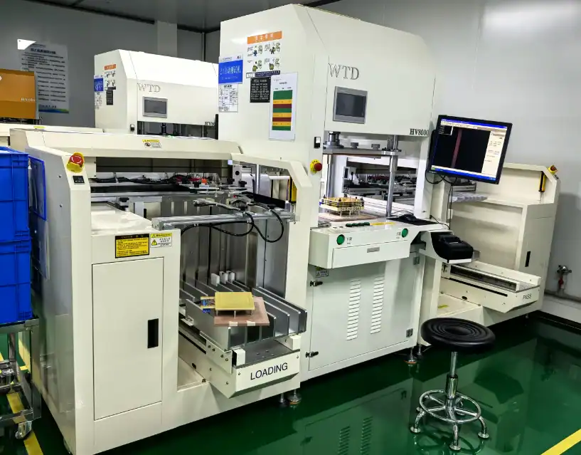
PCB drilling machine in the Shenzhen factory
Drilling equipment at our Shenzhen factory.
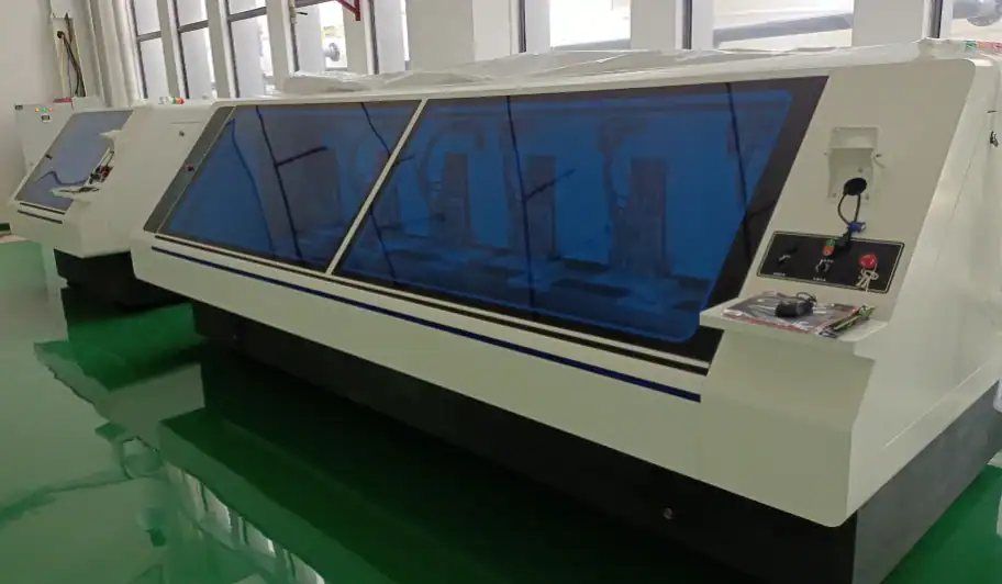
Bare-board electrical test equipment in the Shenzhen factory
Electrical test equipment at our Shenzhen factory.
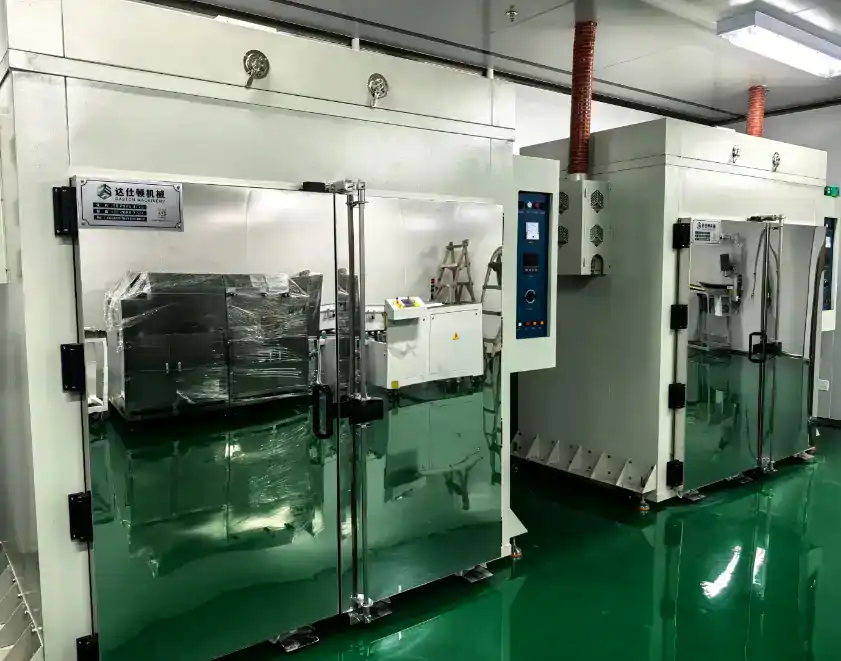
Two industrial ovens in the Shenzhen factory
Industrial ovens at our Shenzhen factory.

Checks available on 4-layer orders

Every board is 100% electrically tested (flying probe or fixture) and passes automated optical inspection (AOI). X-ray is available on request.

On ENIG boards, nickel and gold thickness is measured by XRF on every lot, and the readings can ship with the boards. Bare-board solderability testing is done in-house.

Ask for the inspection scope and records you need with your order.

Pricing

What sets the price of a 4-layer board

Board size, panel use and quantity
How many boards fit a production panel, and how many boards share the setup cost.
Material and finished thickness
Standard FR-4 or a named grade, and the core and prepreg needed to reach your thickness.
Copper weight
Heavier copper needs wider features and can add processing work.
Surface finish
The selected finish changes the process cost; hard gold fingers add local plating and, when specified, bevelling.
Via treatment
Resin-plugged and VIPPO vias add filling, planarizing and plating steps.
Impedance control
Reviewing the construction and drawn geometry for the controlled nets.
Acceptance class and records
Acceptance class, test coverage and the records requested affect the quoted scope.

Send these for an accurate quote

  • Gerber or ODB++ data with drill files
  • A fabrication drawing or note: layer order, thickness, copper, material, finish and colours
  • An impedance table, if you have controlled nets
  • Quantity, plus your panel drawing if you want panels (we build to your panel design)
  • The records you need with delivery

Missing something? Send what you have and we will ask for the rest. Assembly is quoted separately. There is no strict MOQ.

Send files for a quote

Lead time

From files to delivery

Under 1 m²5 days
1–5 m²7 days
Above 5 m²12 days
Expedited from24 hours

What changes the lead time

Board area and quantity, material availability, finish, VIPPO or impedance requirements, and Class 3 acceptance all change the schedule, and so does each round of open questions. Standard 4-layer lead time is 5 days under 1 m², 7 days for 1–5 m² and 12 days above 5 m²; expedited builds from 24 hours. Include your required delivery date so we can check the available schedule.

  1. File review

    A CAM engineer checks layer order, drill, outline and your notes, and sends questions if anything is unclear.

  2. Quote

    Bare PCB quotes are typically sent within 2 hours of receiving complete Gerber files. Review the price, construction, finish, acceptance class, records and lead time for your order.

  3. Engineering release

    You confirm the order and approve any construction or line-width proposal.

  4. Fabrication

    Inner layers are imaged and inspected, then laminated. Holes are drilled and plated, outer layers etched, and solder mask, legend and finish applied.

  5. Test and inspection

    The tests and records listed in your quote, such as electrical test and ENIG thickness readings.

  6. Packing and shipment

    Boards are vacuum-sealed with desiccant in ESD-safe bags and ship from our Shenzhen factory by DHL, FedEx or UPS, typically 3–5 days door to door.

FAQ

4-layer PCB buying questions

Can I order before my stackup is final?

Yes. Send the files with the thickness target and anything else you have fixed, and mark the rest as open. We propose a construction for the open items, and you approve it before production starts.

What finished thickness can you build for a 4-layer board?

We build to the finished thickness you specify. Give the target and the tolerance you need. If the core and prepreg schedule is open, we propose one that meets the target.

How do you handle controlled impedance?

List each controlled net class with its target, tolerance, signal layer, reference layer, and drawn width and spacing. We review the construction and drawn geometry, and ask you to approve any proposed change before fabrication. Our standard tolerance is ±5%, and controlled-impedance orders ship with a TDR test report.

Which inspections and records can I request?

Every board is 100% electrically tested and passes AOI; X-ray is available on request. Ask us to confirm the checks and records included in your quote. On ENIG boards we measure nickel and gold thickness by XRF on every lot and can ship the readings with the boards. You can also specify IPC Class 2 or Class 3 acceptance.

What files do you need for a quote?

Gerber or ODB++ data with drill files, plus a fabrication drawing or note with layer order, thickness, copper, material, finish and colours. Add the quantity, an impedance table if you have controlled nets, and a panel drawing if you want panels.

Where are the boards made and shipped from?

In our factory in Shenzhen, China. The boards are of Chinese origin and ship from China.

Can you assemble the boards as well?

Yes. PCB assembly is available as a separate quote. This page covers bare 4-layer boards, so mention it in your note if you need assembly.

Are QueenEMS and Queenpcb Limited the same company?

Yes. Queenpcb Limited is the same company, and you may see that name on some documents.

Ready to quote

Send your 4-layer files

Add a note or one ZIP with your Gerbers, drill files and drawing. If you used the layer plan tool, click “Add to my request” to place its summary in this form. You can edit it before sending.

Helpful details to include

  • Thickness, copper weights and surface finish
  • Impedance targets and any via treatment
  • Quantity, acceptance class and delivery date
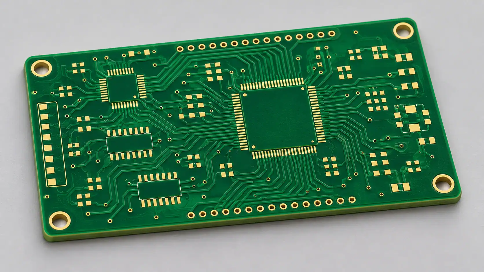
Illustrative bare 4-layer PCB with green solder mask and gold-finished pads.

Request a review and quote

Only email is required.

Up to 50 MB: ZIP, RAR or Gerber/drill files. Put PDF drawings, ODB++ data or several files into one ZIP or RAR. The file uploads as soon as you select it.