
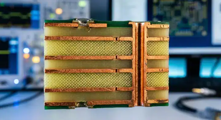
Quick answer: A PCB Stack-Up Design is ready for fabrication only when the proposed layer construction and the routed design agree. Identify layer order, plane assignments, copper, pressed dielectric thickness, material, finished thickness, and any controlled-impedance structures. Ask the fabricator to return a buildable construction; let engineering approve any change to geometry, material, or reference plane before release.
Table of Contents
- What Should a PCB Stack-Up Design Include?
- How Do Layer Count and Reference Planes Affect Signals?
- When Should You Move From 4 Layers to 6 Layers?
- How Should Materials and Dielectrics Be Chosen?
- How Do You Control Impedance Without Guessing?
- What Stack-Up Mistakes Cause Warpage or EMI?
- How Do BGA, HDI, and Vias Change the Stack-Up?
- What Should You Send Before Fabrication Release?
- FAQ
A layer diagram shows intent; it does not prove that a factory can build the assumed dielectric and copper construction. The designer first needs continuous return paths and workable routing channels. The fabricator then has to map those requirements to available cores, prepregs, copper foils, and process tolerances. This page owns that design-to-construction review. The separate supplier stack-up sign-off guide covers the later approval record.
The safest workflow is to define the design intent first, then let the fabricator return a buildable stack-up using available cores, prepregs, copper foils, and process tolerances. That returned stack-up should go back into the impedance solver before production release.
What Should a PCB Stack-Up Design Include?
A complete PCB Stack-Up Design should include every physical and electrical assumption the fabricator needs to build the board consistently. At minimum, define the layer order, signal and plane layers, finished thickness target, copper weights, dielectric materials, impedance-controlled nets, and the acceptance or coupon method.
A useful stack-up package separates design intent from factory proposal. Your layout note might say that Layer 1 requires 50-ohm single-ended routing, but the fabricator should return the actual dielectric thickness, copper type, trace adjustment, and tolerance it can hold with its materials.
| Stack-up item | Why it matters | What to confirm |
|---|---|---|
| Layer order | Controls routing, return path, shielding, and symmetry | Signal, plane, power, and mixed-signal layer names |
| Dielectric thickness | Drives impedance and finished thickness | Pressed thickness, not only catalog prepreg thickness |
| Copper weight and plating | Changes trace geometry, heat, current, and etching limits | Base copper, finished copper, and line-width compensation |
| Material family | Affects Tg, Dk, Df, CAF risk, loss, and assembly margin | Approved laminate, prepreg, or equivalent rule |
| Impedance targets | Links routing to electrical performance | Net class, layer, target value, tolerance, and coupon plan |
For complex boards, connect the stack-up with the broader multilayer PCB fabrication requirements instead of treating it as a standalone drawing.
How Do Layer Count and Reference Planes Affect Signals?
Layer count affects signal quality because every fast signal needs a stable reference plane and a short return-current path. A trace that crosses a plane split, changes layers without a nearby stitching path, or runs beside a noisy power region can fail even when its calculated trace width looks correct.
A two-layer board can work for simple low-speed electronics, but it gives limited control over return paths and electromagnetic interference. Four layers usually allow one solid ground plane and better routing discipline. Six or more layers can provide better separation for dense components, power distribution, and high-speed interfaces when the added cost is justified.
Reference planes are especially important when a signal changes layers through a via. If the return current has to detour around a split or move between distant planes, the via transition becomes part of the signal path problem, not just a mechanical connection.
When Should You Move From 4 Layers to 6 Layers?
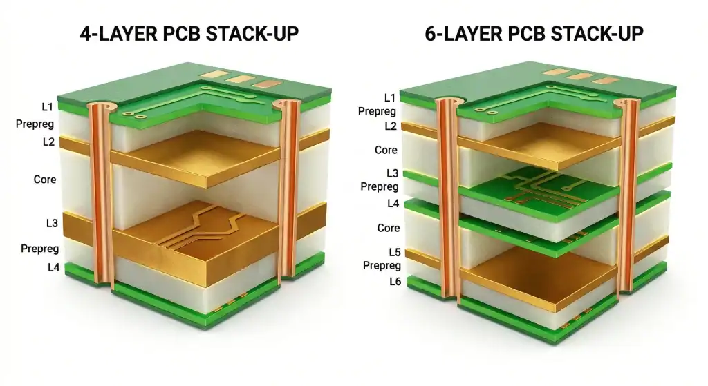
Move from 4 layers to 6 layers when the extra planes solve a real routing, return-path, power-integrity, BGA escape, EMI, or manufacturability problem. Do not upgrade only because a board looks complex, and do not stay at 4 layers if doing so forces chopped ground, narrow neck-downs, or uncontrolled high-speed routing.
A practical test is simple: can the critical traces route over continuous reference planes with enough spacing, escape room, and power distribution? If not, a 6-layer stack-up may reduce design risk even if the bare board costs more.
| Design condition | 4-layer risk | 6-layer benefit |
|---|---|---|
| Dense BGA or fine-pitch IC | Escape routing cuts planes or forces tight spacing | More routing channels and cleaner reference-plane planning |
| USB, Ethernet, RF, or fast clocks | Return path and impedance control become harder | Better plane proximity and controlled routing layers |
| Noisy power conversion | Power loops may share space with sensitive signals | Cleaner separation between power, ground, and signal layers |
| Strict EMI target | Outer-layer routing can radiate more easily | Buried signals and adjacent planes can improve shielding |
If the decision is mainly cost-driven, compare the stack-up with the board size, assembly density, yield risk, and debug time. The QueenEMS 4-layer vs 6-layer PCB cost and EMI article can help frame that trade-off.
How Should Materials and Dielectrics Be Chosen?
Materials and dielectrics should be chosen from the electrical requirement, assembly exposure, board thickness, and fabricator availability. A generic FR-4 note is often too loose for controlled impedance, lead-free reflow margin, high layer count, or low-loss channels.
Do not use a single catalog Dk value as a substitute for the proposed construction. Resin content, glass style, frequency, copper profile, and pressed dielectric thickness affect the model. Ask which material and Dk assumptions the fabricator used, then update the field-solver model before approving any trace change. Altium’s layer-stack documentation describes how material and layer assignments connect to impedance profiles.
For standard digital boards, the material decision may be about Tg class, CAF resistance, and lead-free assembly reliability. For RF or very high-speed channels, the decision may shift toward loss tangent, copper profile, thickness availability, and validated impedance/loss coupons. QueenEMS’ PCB material selector and FR-4 material guide give separate context for those choices.
How Do You Control Impedance Without Guessing?
You control impedance by tying each target value to a layer, geometry, dielectric thickness, reference plane, copper thickness, and manufacturing tolerance. A note that says only “50 ohms” is not enough because the fabricator still needs to know which traces, which layers, and which measurement method apply.
Start with your routing constraints, then request a fabricator-adjusted stack-up before production. The returned version may change trace width, spacing, prepreg choice, or copper assumptions. Feed those changes back into the layout and solver instead of treating them as paperwork.
- Identify each controlled-impedance net class and target value.
- State whether the trace is microstrip, stripline, coplanar, or differential.
- Confirm the reference plane for every routed segment.
- Review via transitions, stitching vias, and plane changes.
- Require coupon, TDR, or other agreed evidence when the interface justifies it.
For deeper impedance-specific checks, connect this page with the QueenEMS controlled impedance PCB design and manufacturing guide.
What Stack-Up Mistakes Cause Warpage or EMI?
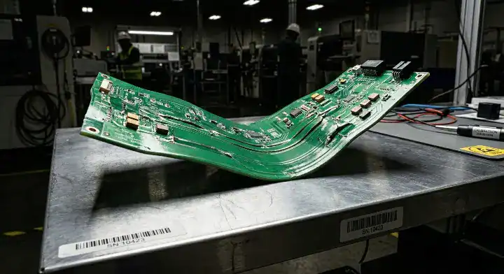
The stack-up mistakes most likely to cause trouble are asymmetry, broken reference planes, unclear material substitutions, unrealistic finished thickness, and copper distribution that ignores lamination behavior. These issues can show up as bow and twist, impedance drift, poor EMI performance, solder-joint stress, or extra engineering questions before fabrication.
Related stackup check: If the design uses mixed board thickness or controlled-depth mechanical features, confirm the stepped-thickness PCB stackup requirements before fabrication release.
Symmetry matters because the board is pressed and then heated again during assembly. If copper weight, dielectric thickness, or material type is very different above and below the centerline, the board can move more during fabrication and reflow.
| Red flag | Better stack-up instruction | Why it helps |
|---|---|---|
| Generic “FR-4” note | Name the material class and substitution approval rule | Reduces silent material changes |
| High-speed traces crossing plane splits | Keep a continuous reference plane under the route | Protects return-current path |
| Unbalanced copper or dielectric buildup | Mirror major copper and dielectric structures around the center | Reduces bow, twist, and assembly stress |
| Unclear impedance notes | List net class, layer, target, tolerance, and coupon plan | Turns the requirement into a measurable build instruction |
For boards already showing bending problems, the QueenEMS article on PCB warping causes and prevention covers the mechanical side in more detail.
How Do BGA, HDI, and Vias Change the Stack-Up?
BGA, HDI, and via choices change the stack-up because they define escape routing, drill structures, plane continuity, and lamination complexity. A dense BGA can force extra routing layers, microvias, via-in-pad, or thinner dielectrics that would not be needed on a simpler connector board.
Rigid-flex stackup note: If the stackup includes flex zones, adhesive windows, or selective bonding, add rigid-flex no-flow prepreg lamination control to the release checklist.
The HDI PCB Guide puts the stack-up decision in the wider HDI context, including microvia routing density, build-up sequence, and the evidence a fabricator needs before release.
Before locking the stack-up, check whether the BGA escape needs dog-bone fanout, via-in-pad, blind/buried vias, or sequential lamination. Each option changes cost, reliability review, inspection, and the kind of notes the fabricator needs. The QueenEMS BGA pad and escape-routing article is the better place for package-level layout detail.
Via transitions also matter electrically. A high-speed route that changes layers should keep its return path close, especially when moving between reference planes. Stitching vias, ground vias near connector transitions, and clean plane assignment can matter as much as the nominal impedance number.
What Should You Send Before Fabrication Release?
Before fabrication release, send a controlled package that lets the supplier confirm the stack-up instead of guessing. Include the Gerbers or ODB++/IPC-2581 package, drill files, fabrication drawing, target finished thickness, copper weights, material requirements, impedance table, critical nets, surface finish, assembly profile, and substitution rule.
Ask the fabricator to return a proposed construction with cores, prepregs, pressed thicknesses, calculated geometry, coupon plan, and open engineering questions. Compare that proposal with the released layout. If a reference plane moves or the required trace width no longer fits a BGA escape, the correct action is a layout review, not a silent CAM edit.
Engineering analysis: Consider a routed L3 differential pair referenced to L2 and L4. If a new prepreg construction changes its separation from a plane, the original width-and-spacing calculation no longer describes the proposed board. Engineering should compare the returned stack-up with the route, rerun the impedance model, and approve a revised file set or request another buildable construction. This is a review example, not a claimed QueenEMS production case.
If your design is still open, send the current stack-up, critical interfaces, impedance table, material preference, and assembly requirements through QueenEMS’ free PCB DFM check. The useful output is a buildable stack-up proposal and a list of unresolved engineering questions, not a generic approval.
FAQ
Can I use a standard PCB stack-up from an online calculator? Yes, but only as a starting point. The calculator does not know your fabricator’s pressed dielectric thickness, copper treatment, material inventory, or line-width compensation.
What’s the best PCB Stack-Up Design for a 4-layer board? A common starting point is signal, ground, power, signal, but the best structure depends on routing density, return paths, power noise, connectors, and assembly constraints.
How do I know if my PCB needs controlled impedance? Use controlled impedance when an interface, RF path, fast edge rate, or compliance requirement depends on predictable transmission-line behavior. The requirement should be tied to specific nets and layers, not written as a generic board note.
Can the fabricator change my PCB Stack-Up Design? Yes, but the change should be returned for engineering approval before production. Material, dielectric, copper, and trace adjustments can affect impedance, thickness, reliability, and compliance.
Written by the QueenEMS Engineering Team.
For a production quotation, send QueenEMS the fabrication files, proposed stack-up, material callout, impedance table, assembly profile, quantity, and any substitution restrictions through the QueenEMS quotation request.
Upload your files today · Free DFM check before production · Ship worldwide
Get your PCB prototypes in as fast as 24 hours. We handle FR4, Rogers, and hybrid boards up to 40 layers in volume production, with advanced builds subject to engineering review — free prototypes for 2–4 layer FR-4 boards, no minimum order.
Just upload your Gerber + BOM — we source every part, assemble, and inspect (AOI + X‑Ray) so you don't have to chase suppliers. Boards ship in as fast as 24 hours.