QUOTE NOW

12-layer bare PCB fabrication, Shenzhen

12 Layer PCB Manufacturer

QueenEMS fabricates 12-layer bare boards in Shenzhen. Our CAM engineers, who prepare manufacturing data, review power domains, drill depth and construction before we quote.

A 12-layer power map with unnamed domains brings questions before quoting. Name each power domain by layer, and cite the approved construction revision on repeat orders.

Use the form for a quote, or compare the two layer allocations below first.

Request a review and quote

Only email is required.

Up to 50 MB: ZIP, RAR or Gerber/drill files. Put PDF drawings, ODB++ data or several files into one ZIP or RAR. The file uploads as soon as you select it.

2 h

Bare PCB quotes are typically sent within 2 hours of receiving complete Gerber files.

10 days

Standard lead time for boards above 10 layers, up to 5 m²; expedited builds from 72 hours.

±5%

Standard impedance tolerance; TDR test report supplied with controlled-impedance orders.

100%

Electrical test (flying probe or fixture) and AOI on every board.

Before you send files

Three gaps to close before fabrication

Power shapes without domain names

Power-layer artwork shows copper shapes and gaps. If the data does not identify their nets, a fabricator cannot reliably map each shape to its power rail. Name the domains and specify the copper weight on each layer so we can review the build against your requirements.

Illustrative fab note: L4 carries 1V0 and 1V8 as separate shapes; L9 carries 3V3; domain names per layer map PDF; inner copper weights per drawing.

Check: Send a layer map that names each power domain by layer with its copper weight, or ODB++ data that carries net names.
Thickness and hole size stated apart

On a 12-layer board, a through hole runs the full finished thickness. The drill used before plating is larger than the finished hole, because plating adds copper inside the barrel. With both finished thickness and the smallest finished plated hole, our engineers can review the drill and plating process that depth actually needs. If either value changes later, that review is repeated.

Illustrative fab note: finished thickness and tolerance per drawing; smallest finished plated hole per drill table; through holes only.

Check: State finished thickness with tolerance, the smallest finished plated hole, and which holes run through the full board.

Repeat orders tied to Gerbers only

The approved construction records the cores, prepreg, copper weights and laminate behind every calculated trace width. A repeat order that cites only Gerbers gives no approved build to quote against, so CAM sends the construction back for approval. Citing the revision lets us build the same construction again.

Illustrative fab note: build to approved construction revision B; same laminate; confirm impedance record and ENIG XRF readings with the quote.

Check: Cite the approved construction revision on every repeat order, and ask us to confirm the records you need with the quote.

Our process

How CAM reviews a 12-layer order

CAM review checks whether your files and construction can be built as described. Open items come back to you as written questions or proposals for approval.

Send your files for review

  1. Match domains to copper

    We compare your layer map with the artwork and flag any power shape that has no named domain.

  2. Check the physical build

    We review layer order and copper distribution across both halves of the board. Mirrored role labels do not show whether the copper is physically balanced.

  3. Review drill depth and hole size

    We review the actual drill depth, drill diameter before plating and finished hole requirements together. The drill spans in your files identify which layers each hole connects.

  4. Keep or complete the construction

    We review your specified construction and propose changes only where needed, for your approval. A core is cured laminate; prepreg is the resin and glass bonding sheet used in lamination.

  5. Calculate nets and record the revision

    We review impedance geometry for the net classes you list and record the approved construction revision. Your design team checks the complete signal and power behaviour.

Match your board

What we build at twelve layers

For a twelve-layer prototype or production order, include the details that match your board below.

If three or more rails share a layer
Name each domain on the layer map and specify its copper weight. CAM checks each power shape against the domain named on your map.
If the board must fit a connector or enclosure
State finished thickness and tolerance early. The drill and plating review depends on that thickness and your smallest finished hole.
If an earlier lot must be repeated
Cite the approved construction revision and laminate. We build to that record and return any required change for your approval.
If some nets need controlled impedance
List each net with its target, layers, reference planes, and CAD width and gap. We calculate geometry on the approved construction.
If your drawing fixes the construction
Send the construction and revision. CAM reviews material availability and buildability; any proposed change needs your approval.

Layer roles

Compare two 12-layer role plans

Both plans use twelve copper layers. A reference plane is the solid copper layer beside a signal that carries its return current. Dielectric thickness and copper weight come from the approved construction.

SignalGroundPower

Plan A

Signal / Ground / Signal / Power / Signal / Ground / Ground / Signal / Power / Signal / Ground / Signal

  1. L1 Signal
  2. L2 Ground
  3. L3 Signal
  4. L4 Power
  5. L5 Signal
  6. L6 Ground
  7. L7 Ground
  8. L8 Signal
  9. L9 Power
  10. L10 Signal
  11. L11 Ground
  12. L12 Signal

Six signal layers, four ground layers and two power planes. L1 and L12 reference grounds on L2 and L11. L3, L5, L8 and L10 each sit beside one power plane. L6 and L7 are grounds at the centre.

Plan for: If a signal uses the L4 or L9 power plane as its reference, review the return path and decoupling in your layout. Mirrored roles do not establish physical copper balance or dielectric spacing.

Plan B

Signal / Ground / Power / Power / Signal / Ground / Ground / Signal / Power / Power / Ground / Signal

  1. L1 Signal
  2. L2 Ground
  3. L3 Power
  4. L4 Power
  5. L5 Signal
  6. L6 Ground
  7. L7 Ground
  8. L8 Signal
  9. L9 Power
  10. L10 Power
  11. L11 Ground
  12. L12 Signal

Four signal layers, four ground layers and four power planes. This plan gives more plane area to power domains. L3 and L4 are adjacent power layers, as are L9 and L10. L5 and L8 each sit between a power plane and a ground.

Plan for: Domains on L3 and L4, and on L9 and L10, face each other and couple. Mark which ones overlap on your layer map. Role labels do not prove copper balance or dielectric thickness.

Layer roles are examples; dimensions and construction need approval. For design trade-offs, see our PCB stack-up design guide. Use the supplier stackup sign-off guide when checking a proposed construction.

Add your layer plan to the request

Every field is optional. The tool formats a brief for CAM review. It does not calculate impedance, check the design or submit a request.

No choices yet. When you pick a layer plan, a short note about what it asks you to plan for appears here.

Specifications

12-layer capability

These figures apply after CAM review of your files and construction. Feature combinations are confirmed per design.

Layers and construction
ItemCapabilityWhat to send us
Layer count12 layers on this page; standard multilayer up to 24 layers, up to 32 layers reviewed per designLayer count and role of each layer
ConstructionA construction fixed on your drawing is reviewed and kept; open items are proposed for approvalYour construction and revision, or targets to work from
Finished thicknessPer approved constructionTarget thickness and tolerance
Heavy copper inner layersUp to 12 oz, subject to stack-up reviewCopper weight on each layer
Traces, holes and impedance
ItemCapabilityWhat to send us
Trace and space, standard copper3/3 mil (75 µm)Smallest trace and space by layer
Trace and space, 3 oz copper6/8 milLayers that carry 3 oz copper
Trace and space, 6 oz and heavier9/14 milLayers and copper weight
Controlled impedance±5% standard tolerance; TDR test report supplied with controlled-impedance ordersNet list with target, layers, reference planes, CAD width and gap
Drilling and platingProcess reviewed from finished thickness and finished hole sizeSmallest finished plated hole and drill spans
Hole position±0.025 mmDrill table and fab drawing
Smallest mechanical drill0.10 mm (4 mil); production minimum confirmed at reviewFinished hole sizes in the drill file
Layer registration±2 milAny tighter registration need on the drawing
Plated hole copper≥20 µm; ≥25 µm when Class 3 is specified; micro-section report availableAcceptance class
Laser microvia0.075 mm on HDI buildsMicrovia spans in the drill table
Via treatmentResin plugging; VIPPO filled and plated overWhich vias need plugging or via in pad
Finish, inspection and acceptance
ItemCapabilityWhat to send us
Inspection100% electrical test (flying probe or fixture) and AOI on every board; X-ray availableAny added tests or records you require
AcceptanceIPC-6012 / IPC-A-600 Class 2 or Class 3, specified per orderRequired class

For other layer counts, see our 4-layer, 6-layer and 8-layer PCB manufacturer pages, or the multilayer PCB manufacturing overview.

Materials

Laminates and surface finishes

Keep the specified laminate and bonding materials with the twelve-layer construction revision. If different materials are used in one build, identify which layers use each system.

Name the material grade or required properties. Tg is the glass transition temperature; Dk describes dielectric permittivity used in impedance modeling. Two materials with equal Tg can still need different impedance geometry. Standard FR-4 (Tg 130–180), high-Tg FR-4, and high-frequency Rogers and PTFE laminates are available.

State whether equivalents are acceptable. We review proposed substitutions against material requirements and impedance geometry, then seek approval for any construction change.

ENIG
Electroless nickel with immersion gold gives flat pads for fine-pitch parts. XRF nickel and gold thickness readings for each lot can accompany the shipment.
ENEPIG
Adds palladium between nickel and gold. Specify it when your assembly process calls for it, such as wire bonding.
OSP
A thin organic coating on bare copper that keeps pads flat. Agree storage time and reflow cycles with your assembler.
HASL
Hot air solder leveling coats pads with solder. The surface is less flat than ENIG or OSP, so check it against your finest-pitch pads.

Hard gold fingers with bevel, castellated edges and carbon ink are available. Mark their locations on the drawing. Filled and plated-over via-in-pad (VIPPO) is also available; identify the pad vias that need filling and capping. Immersion silver and immersion tin are also available.

Our factory

Inside our Shenzhen factory

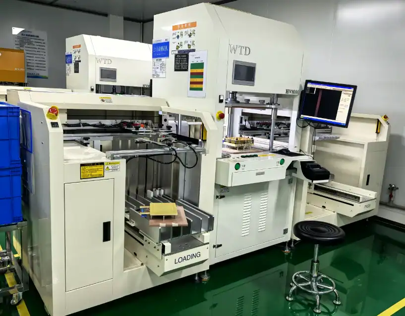
These photos come from our own production floor and show equipment as installed. Production is ISO 9001:2015 and UL certified and RoHS compliant.

  • 30,000 m²Shenzhen factory
  • 480+Staff
  • 20+CAM engineers
  • 50,000+ m²Monthly capacity
Drilling equipment in the Shenzhen factory
Drilling equipment at our Shenzhen factory.

Drilling

Drilling equipment forms the holes in your drill files. Hole position capability is ±0.025 mm.

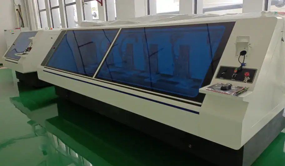
Bare-board electrical test equipment in the Shenzhen factory
Electrical test equipment at our Shenzhen factory.

Electrical test

Every finished board is 100% electrically tested for opens and shorts, by flying probe or test fixture.

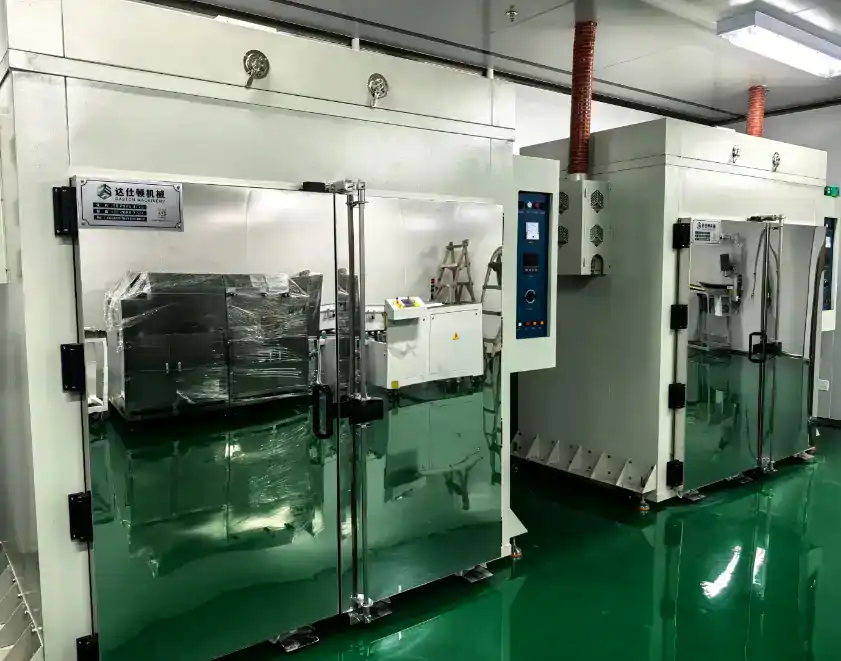
Two industrial ovens in the Shenzhen factory
Industrial ovens at our Shenzhen factory.

Industrial ovens

Industrial ovens in our production area. Ask CAM which process steps your construction involves.

Choose records to suit the board. For controlled nets, ask how impedance will be verified and recorded. For ENIG, ask for XRF readings. For repeat orders, ask that records cite the construction revision. Ask us to confirm these with the quote.

Pricing

What drives a 12-layer quote

Price follows the construction and the scope you request. There is no strict MOQ; we build from prototype quantities to volume production.

Construction
More cores, prepreg sheets and copper layers, and any heavy copper, raise material and lamination cost.
Drill depth and spans
Small finished holes in a thick board need closer drill and plating control. Blind or buried spans may change the lamination route, depending on the layers they connect.
Via treatment and finish
Resin plugging, VIPPO, the surface finish and gold fingers each add process steps.
Acceptance and test coverage
Class 3 acceptance and test coverage beyond the agreed scope add inspection work. Ask which of your requested records would need added inspection.

Include with your request

  • Gerber or ODB++ files with drill files
  • Power-domain layer map with copper weights
  • Finished thickness, tolerance and smallest finished plated hole
  • Controlled-net list, if any
  • Laminate, finish, acceptance class and construction revision
  • Quantity and the records you need

Ask us to confirm the construction, test scope, records and delivery date with your quote.

Request a quote

Lead time

From files to shipment

Up to 5 m²10 days
Above 5 m²15 days
Expedited from72 hours

Bare PCB quotes are typically sent within 2 hours of receiving complete Gerber files. Standard lead time for boards above 10 layers is 10 days up to 5 m² and 15 days above 5 m²; expedited builds from 72 hours. Special materials and features are confirmed in the quote.

  1. Send files

    Email Gerbers, drill files, the layer map and any revision. Email is the only required field.

  2. CAM review

    CAM matches domains to copper, reviews drill depth and hole size, and checks the construction.

  3. Questions and quote

    You receive open questions, any proposed items and the quote scope you asked us to confirm.

  4. Approve the revision

    You approve the construction revision and any substitution before production starts.

  5. Fabricate and inspect

    Boards are built and inspected to the agreed acceptance class and test scope.

  6. Ship from Shenzhen

    Boards are vacuum-sealed with desiccant in ESD-safe bags and ship from China by DHL, FedEx or UPS, typically 3–5 days door to door.

Confirm the delivery date

Give your required arrival date and destination. Material availability, hole spans, via treatment, quantity and open review questions affect the schedule. Assembly can be quoted separately with a BOM.

FAQ

12-layer PCB buying questions

What should a power-domain layer map show?

For each layer, name the domains it carries, their copper weight, and which shapes overlap domains on the next layer. ODB++ data with net names can serve the same purpose.

Does a 12-layer board need HDI or extra lamination?

Layer count alone does not require high-density interconnect (HDI), microvias or sequential lamination. Through-hole and partial-depth hole spans have different process requirements; CAM reviews the construction and drill sequence for your design.

Why give finished thickness and finished hole size together?

Together they let our engineers review the drill diameter and plating process for the full hole depth. The drill used before plating is larger than the finished hole.

Will you change the construction on my drawing?

We review it and keep it. If an item cannot be built, we propose a change in writing as a new revision for your approval.

How do repeat orders stay on the same build?

Cite the approved construction revision on the order. We build to that record, including laminate, cores, prepreg and copper weights.

Do you validate signal or power integrity?

Our manufacturing review covers buildability and impedance geometry. Your design team checks return paths, decoupling and power distribution in the complete layout.

Which records can I request?

Every board is 100% electrically tested. Controlled-impedance orders ship with a TDR report, ENIG lots with XRF nickel and gold readings, and micro-section reports are available. Ask us to list them in the quote.

Can you assemble the boards as well?

Yes. Assembly is quoted separately from the bare board and needs a BOM with the design files.

Ready to quote

Send your 12-layer files

Attach Gerbers, drill files and a power-domain layer map, or describe the board first. Only email is required. A named layer map and construction revision give CAM fewer questions to send back.

Helpful details to include

  • Thickness, copper weights and surface finish
  • Impedance targets and any via treatment
  • Quantity, acceptance class and delivery date
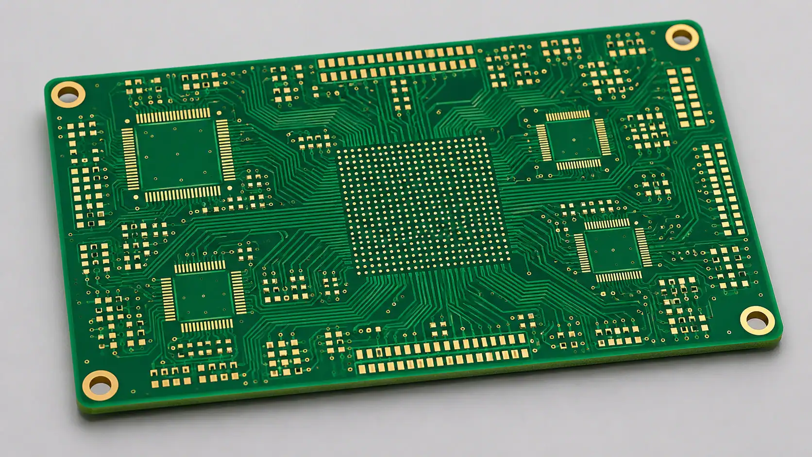
Illustrative bare 12-layer PCB with green solder mask and gold-finished pads.

Request a review and quote

Only email is required.

Up to 50 MB: ZIP, RAR or Gerber/drill files. Put PDF drawings, ODB++ data or several files into one ZIP or RAR. The file uploads as soon as you select it.