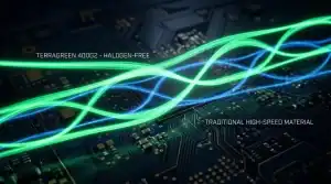
For decades, hardware engineers accepted a painful trade-off: if your design required halogen-free environmental compliance, you had to sacrifice electrical...
Pushing millimeter-wave designs into mass production requires balancing electrical performance with fabrication reality. This engineering Astra MT77 guide explains how...
Navigating material allocation in 2026 requires understanding the exact trade-offs between top-tier PCB laminates. This M8 CCL comparison provides a...
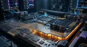
Hardware engineers frequently face severe signal integrity bottlenecks and prolonged material allocation delays when designing 112G and 224G AI architectures....
Many hardware engineering teams designing infrastructure around the latest AI platforms struggle to define the exact bare-board specifications required to...