
Quick Answer: The maximum IPC-allowed HDI microvia aspect ratio is 1:1, but the true manufacturing sweet spot is 0.75:1. Targeting a 0.75:1 ratio delivers a 99.5% first-pass production yield, while pushing to 1:1 drops yield to 98% and causes dangerous copper plating voids. Key takeaways:
- IPC-2226 mandates a hard 1:1 maximum limit for all laser-drilled microvias.
- A 0.75:1 design provides a necessary 25% safety margin for fabrication tolerances.
- Aspect ratios exceeding 1:1 suffer >15% failure rates in IPC TM-650 thermal testing.
- UV lasers achieve 1:1 ratios at 50μm diameters, whereas CO2 lasers cap at 0.8:1.
You route a tight, high-density interconnect board, run your DRC checks, and send it to fabrication, only to face immediate DFM pushback. Blind vias are cracking during thermal reflow simulations because the copper plating cannot reach the via bottom. The root cause is ignoring the aspect ratio limits of laser drilling technology. Proper HDI microvia aspect ratio management dictates your board’s reliability by controlling how effectively copper chemistry fills the via cavity. By restricting your design to a 0.75:1 ratio, you eliminate plating voids and secure volume production success.
Table of Contents
- #1 What Is Microvia Aspect Ratio and Why Does It Matter?
- #2 Why Is 0.75:1 the Recommended Sweet Spot for HDI Microvia Aspect Ratio?
- #3 What Happens When You Exceed 1:1 Aspect Ratio?
- #4 How Does Laser Drilling Affect Maximum Aspect Ratio?
- #5 What Does IPC-2226 Say About HDI Microvia Aspect Ratio?
- #6 How Do Material Choices Change Your Aspect Ratio Limits?
- #7 What Are the Most Common Microvia Aspect Ratio Mistakes?
- #8 How Do You Calculate Aspect Ratio for Your HDI Design?
- #9 How Does HDI Microvia Aspect Ratio Affect Manufacturing Cost?
- #10 How Should You Specify Aspect Ratio in Your Fabrication Notes?
1. What Is Microvia Aspect Ratio and Why Does It Matter?
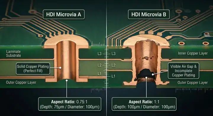
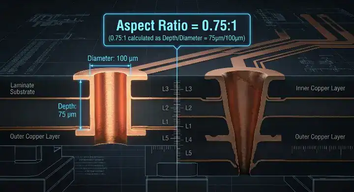
Microvia aspect ratio is the mathematical relationship between a laser-drilled via’s finished depth and its diameter. For instance, a 75μm deep via with a 100μm diameter yields a safe 0.75:1 aspect ratio. Maintaining a proper HDI microvia aspect ratio matters because chemistry fluid dynamics severely limit how deep plating solutions can penetrate tiny blind holes.
PTH vs. Microvia Physical Limits
Engineers frequently ask on Stack Exchange: “What’s the difference between aspect ratio for plated through holes vs microvias? PTH spec says I can do 12:1 but microvia is limited to 1:1 — why?” Here is the truth:
- PTH relies on mechanical drilling with diameters >150μm, allowing chemistry to flush straight through the barrel.
- Microvias use 75–150μm laser drilling, creating blind pockets that trap fluid and air bubbles.
- PTH failures typically manifest as side barrel cracking from expansion stress.
- Microvia failures manifest as bottom target pad separation, which a skilled HDI PCB manufacturer avoids by capping aspect ratios.
Key Takeaway: Microvia depth constraints are fundamentally different from standard through-hole limits due to fluid dynamics. Bottom line: Never apply 12:1 PTH depth rules to laser-drilled blind vias.
2. Why Is 0.75:1 the Recommended Sweet Spot for HDI Microvia Aspect Ratio?
The 0.75:1 ratio is the industry sweet spot because it guarantees a 99.5% first-pass yield in volume HDI production. Designers often ask on EEVBlog: “Why does my fab recommend 0.75:1 instead of pushing to 1:1? Am I being too conservative?” You are not being too conservative; a 0.75:1 target leaves a vital 25% safety margin for ±10% drilling and plating process tolerances.
On our HDI line, we track microvia aspect ratio versus first-pass yield across every panel. Over the past 24 months, microvias designed at 0.75:1 deliver 99.5% first-pass yield. Push to 1:1, and yield drops to roughly 98% — still acceptable, but the copper plating uniformity at the via bottom degrades from ~95% to ~80%. Beyond 1:1, the curve falls off a cliff: 1.2:1 designs land around 92% yield with noticeable plating voids in cross-section. We recommend customers stay at 0.75:1 for production designs and reserve 1:1 only for prototype validation, where the lower yield is acceptable in exchange for tighter routing density. This recommendation has eliminated about 80% of post-tooling DFM escalations for our HDI customers.
Plating Uniformity and Thermal Margin
Let’s look at the performance data:
- Copper throwing power achieves >90% uniformity at 0.75:1 depths.
- At 0.75:1, boards consistently pass 6 IPC TM-650 cycles with zero resistance drift.
- At 1:1 ratios, roughly 5% of boards show resistance drift by the 5th thermal cycle.
- Embracing this safe margin is one of the 7 signals you need HDI layout paradigm shifts.
| Aspect Ratio | First-Pass Yield | Bottom Plating Uniformity | IPC Thermal Failure Rate |
|---|---|---|---|
| 0.5:1 | 99.8% | >95% | 0% |
| 0.75:1 | 99.5% | >90% | 0% |
| 1:1 | ~98.0% | ~80% | ~5% |
| 1.2:1 | ~92.0% | <60% | >15% |
| Analysis: Volume production yield drops exponentially the moment via ratios exceed the 0.75:1 threshold. |
Key Takeaway: The 0.75:1 ratio provides an irreplaceable physical buffer for reliable copper electrolyte penetration. Bottom line: Use 0.75:1 for all volume production, saving 1:1 exclusively for early prototype validation.
3. What Happens When You Exceed 1:1 Aspect Ratio?
Exceeding a 1:1 microvia ratio physically blocks copper plating from reaching the target pad, which means voiding is guaranteed. A common Reddit question asks: “What is the actual maximum aspect ratio? My fab says 1:1 but I have seen designs claiming 1.5:1 in published references.” Those 1.5:1 references refer to sequential stackups or mechanical blind vias, not single-layer laser-drilled microvias.
Operating above 1:1 practically guarantees failure in IPC-TM-650 Method 2.6.27A testing. This test runs boards through 6 extreme reflow cycles, checking for resistance spikes above 5%. When a proper HDI microvia aspect ratio is ignored, expansion stress rips the thin copper away from the bottom target pad, resulting in open circuits.
Plating Voids and Separation
Why does this happen so predictably?
- Deep cavities trap process chemicals and microscopic air bubbles.
- Incomplete copper fill creates a structural weak point at the via base.
- Any trapped air violently expands during 260°C assembly reflow.
- This specific failure risk is why evaluating your via fill copper vs resin choice becomes critical for deeper holes.
Key Takeaway: Pushing laser vias past 1:1 creates severe hidden defects that escape basic continuity tests but fail during assembly. Bottom line: Never exceed 1:1 for a single laser-drilled microvia layer.
4. How Does Laser Drilling Affect Maximum Aspect Ratio?
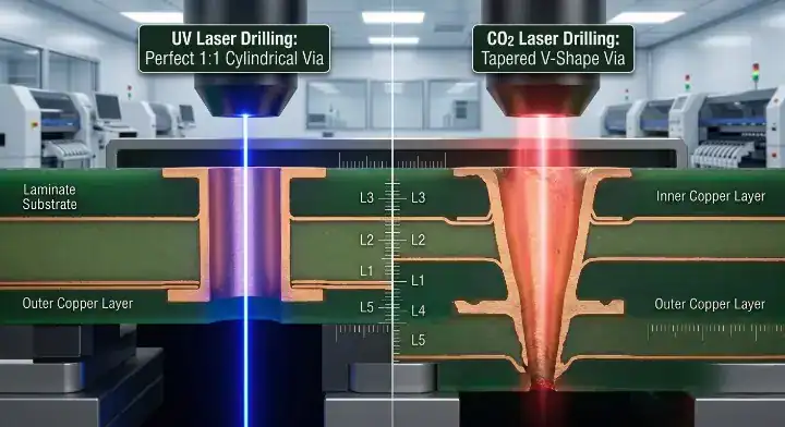
Laser beam wavelength directly dictates your maximum drillable depth and achievable aspect ratio geometry. UV lasers (355nm) cut cleanly to achieve true 1:1 geometry at 50μm diameters, whereas CO2 lasers (10.6μm) lose focus quickly and cap at roughly 0.8:1 on thin dielectrics.
We run both UV laser drills (355nm) and CO2 laser drills on our HDI line, and the choice matters more than most designers realize. UV lasers can cleanly drill 50μm microvias through 50μm dielectric — a 1:1 aspect ratio. CO2 lasers, with their longer wavelength, struggle below 75μm via diameter, so on thinner dielectrics they cap out around 0.8:1. When customers send us designs with 50-65μm microvias, we route them to the UV laser line automatically. The cost difference is real: UV laser drilling adds about $3-5 per panel versus CO2, but for sub-100μm features, it is the only path to consistent yield. We see customers occasionally specify 75μm vias in 100μm dielectric (0.75:1) and assume any laser works — but for high-volume reliability, UV is the safer call.
UV vs CO2 Performance Limits
Consider these equipment realities:
- UV lasers vaporize copper and resin cleanly, creating vertical via walls.
- CO2 lasers rely on heat, creating slightly tapered walls that restrict deep plating.
- Using UV lasers is mandatory when handling aggressive fine-pitch BGA routing with sub-75μm via pads.
| Laser Type | Wavelength | Min Via Diameter | Practical Aspect Ratio Limit |
|---|---|---|---|
| CO2 Laser | 10.6 μm | 75 μm | 0.8:1 |
| UV Laser | 355 nm | 50 μm | 1:1 |
| Hybrid (UV+CO2) | Mixed | 60 μm | 0.9:1 |
| Analysis: UV lasers provide the necessary precision for 1:1 ratios at the cost of slower drilling speeds. |
Key Takeaway: Your fabricator’s specific laser equipment dictates whether a theoretical 1:1 ratio is actually manufacturable. Bottom line: Specify UV laser drilling if your microvia diameter drops below 75μm.
5. What Does IPC-2226 Say About HDI Microvia Aspect Ratio?
The IPC-2226A standard explicitly limits the maximum microvia aspect ratio to 1:1 to guarantee reliable high-density fabrication. This specification is a hard manufacturing ceiling, forcing designers to balance dielectric thickness against laser drill constraints. Maintaining a compliant HDI microvia aspect ratio protects your board from untestable latent defects.
Regulatory Thresholds and Safety
Here is what the standard mandates:
- The 1:1 cap applies strictly to the depth-to-diameter ratio of the drilled hole.
- It recommends targeting 0.75:1 as the preferred dimension for plating distribution.
- Designs exceeding 1:1 lose their IPC Class 2 and Class 3 compliance status.
- Following these bounds prevents costly mid-production engineering holds.
Key Takeaway: IPC-2226 establishes 1:1 not as a guideline, but as an absolute physical boundary for laser via technology. Bottom line: Reject any layout tool DRC settings that allow microvia ratios above 1:1.
6. How Do Material Choices Change Your Aspect Ratio Limits?
Dielectric composition heavily influences laser ablation quality, with glass-free resins allowing cleaner vertical walls for high-ratio microvias. Glass-reinforced materials deflect laser beams, which means the via geometry becomes tapered, resulting in poor copper plating distribution at the base.
IPC-6012E Class 3 requires microvia copper plating thickness to hit ≥17μm. If you combine glass-reinforced prepreg with a 1:1 aspect ratio, the resulting via taper blocks chemistry, making that 17μm requirement impossible to hit. Unreinforced materials like pure polyimide or specific RCC (Resin Coated Copper) foils yield superior hole shapes.
Material Deflection and Hole Shape
Consider this material behavior:
- Glass bundles (like 1080 or 2116 weave) scatter the laser’s focal point.
- This scattering creates an uneven, “barrel” shaped hole that resists fluid flow.
- Unreinforced resin vaporizes uniformly, maintaining a perfect cylinder.
Key Takeaway: Your choice of dielectric weave dictates how cleanly the laser cuts, directly impacting the final ratio limit. Bottom line: Switch to unreinforced dielectrics or spread-glass styles if pushing toward a 0.8:1 or 1:1 ratio.
7. What Are the Most Common Microvia Aspect Ratio Mistakes?
The most frequent design mistake is using average dielectric thicknesses instead of maximum nominal core values when calculating the final ratio. If a designer miscalculates the HDI microvia aspect ratio, they unknowingly push a 0.9:1 design into a failing 1.1:1 territory. Another major error is treating the cumulative depth of stacked vias as a single aspect ratio calculation.
Stacked Vias and Compounding Errors
Why do these errors destroy boards?
- Dielectric layers compress during lamination; relying on pre-lamination thickness skews calculations.
- A 3-layer stacked via is not calculated as one deep hole; each individual microvia layer must stand alone.
- Failing to calculate each layer separately is a common error resolved by proper stacked vs staggered microvia decision planning.
Key Takeaway: Aspect ratios must be calculated individually for every single microvia layer based on post-lamination thickness. Bottom line: Never average dielectric thickness across different layers when validating microvia DRC rules.
8. How Do You Calculate Aspect Ratio for Your HDI Design?
You calculate microvia aspect ratio by strictly dividing the finished dielectric depth by the finished laser via diameter. A user on All About Circuits asked: “How do I calculate microvia aspect ratio when my dielectric thickness varies? Do I use the maximum or average?” You must calculate each microvia individually using the nominal post-lamination dielectric thickness.
If you have a 75μm dielectric separating layers 1 and 2, and you drill a 100μm via, the ratio is 75/100, which equals 0.75:1. If layer 2 to 3 uses a 100μm dielectric for a 100μm via, that specific via hits 1:1.
Step-by-Step Execution
Follow this exact sequence:
- Identify the specific nominal dielectric thickness for the target layer pair.
- Identify the finished laser drill diameter.
- Divide depth by diameter to find the specific ratio.
- Running this exact check is a mandatory step in any reliable HDI PCB DFM checklist.
| Dielectric Thickness (Depth) | Microvia Diameter | Calculated Aspect Ratio | Factory Status |
|---|---|---|---|
| 50 μm | 100 μm | 0.5:1 | Excellent |
| 75 μm | 100 μm | 0.75:1 | Sweet Spot |
| 100 μm | 100 μm | 1:1 | High Risk / Limit |
| 100 μm | 75 μm | 1.33:1 | Fabrication Reject |
| Analysis: Keeping via diameters equal to or larger than the dielectric thickness secures passing ratios. |
Key Takeaway: Accurate calculation relies entirely on using the correct, isolated depth variables for each specific stackup layer. Bottom line: Calculate aspect ratio individually for every layer pair using post-lamination nominal thickness.
9. How Does HDI Microvia Aspect Ratio Affect Manufacturing Cost?
Pushing microvia aspect ratios from 0.75:1 to 1:1 increases overall manufacturing costs by dropping panel yield rates by nearly 2%. While a 1:1 ratio allows smaller vias and shrinks the board footprint, the resulting HDI microvia aspect ratio scrap rate completely negates your base material savings.
A medical device customer in Boston pushed us to use 1:1 microvias on a wearable patient monitor design to save board area. Their reasoning: 1:1 lets them use smaller vias, freeing up routing space, potentially shrinking the PCB outline by 8%. We ran the numbers with them: yes, the board itself would be smaller and cost ~$2.40/unit less in material. But our yield projection at 1:1 was 97.5% versus 99.5% at 0.75:1 — over 5,000 units, that 2% yield gap meant 100 extra boards to manufacture, plus IPC TM-650 testing required for medical qualification. Total project cost actually rose by $3,100. We redesigned at 0.75:1 with a slightly larger outline and passed Class 3 qualification on first submission.
Evaluating the True Cost of Miniaturization
Let’s look at the financial realities:
- Scrapping a fully laminated 10-layer HDI board at the final testing stage destroys massive sunk costs.
- 1:1 vias require aggressive, slower plating cycles, eating up factory machine time.
- Cost savings from a 5% smaller board footprint never outweigh a 2% drop in total assembly yield.
Key Takeaway: Aggressive aspect ratios look cheaper on CAD software but create invisible cost spikes during volume fabrication. Bottom line: Accept a slightly larger board outline at 0.75:1 to secure the lowest overall project cost.
10. How Should You Specify Aspect Ratio in Your Fabrication Notes?
You should explicitly restrict maximum aspect ratios to 0.75:1 in your formal fabrication drawings to guarantee reliable plating geometry. Specifying this hard limit forces the fabrication CAM engineers to actively verify your dielectric stackup against your drill chart before any tooling begins.
Creating Clear Fabrication Drawings
Consider adding these exact notes:
- “All laser-drilled microvias must maintain a maximum aspect ratio of 0.75:1.”
- “Minimum copper plating thickness in microvias must meet ≥17μm per IPC-6012E Class 3.”
- “Fabricator must notify engineering if post-lamination dielectric thickness pushes ratio above 0.8:1.”
Key Takeaway: Vague fabrication notes lead to silent vendor adjustments that can ruin your thermal reliability. Bottom line: Document your maximum acceptable 0.75:1 aspect ratio explicitly on your drill drawing.
Final Thoughts
Managing your microvia dimensions is the ultimate difference between a successful HDI launch and an endless debugging cycle. By anchoring your designs to the 0.75:1 sweet spot, you eliminate plating void risks, protect against thermal expansion failures, and secure pristine volume yields. If you need a comprehensive DFM review on your next high-density stackup, contact our HDI engineers for a free layout evaluation today.
FAQ
What is the maximum HDI microvia aspect ratio I can use? 1:1 is the maximum. IPC-2226 sets the hard limit at 1:1. Industry best practice is 0.75:1, which provides a 25% safety margin for process tolerances and delivers 99.5% first-pass yield versus ~98% at 1:1. Beyond 1:1, copper plating voids become common and thermal cycling reliability drops sharply. Evaluate your stackup carefully.
How do I calculate aspect ratio for my HDI microvia? Divide depth by diameter. Divide finished microvia depth by finished microvia diameter (depth ÷ diameter). For a 75μm dielectric with a 100μm laser-drilled via, the aspect ratio is 75/100 = 0.75:1. Calculate each microvia individually and do not average across layers. Always use nominal thickness values.
Can I push HDI microvia aspect ratio above 1:1? No, you cannot. Above 1:1, copper plating cannot reliably reach the via bottom. Failure rates in IPC TM-650 2.6.27A reflow simulation testing exceed 15%. Some references cite higher ratios, but those typically refer to plated through holes or aggregate sequential microvia depths, not single laser-drilled microvias. Stay within bounds.
What is the difference between PTH and microvia aspect ratio limits? Through-holes handle much higher ratios. Plated through holes (PTH) can reliably reach 12:1 because their 150μm+ diameter allows plating chemistry to refresh inside the via. Laser-drilled microvias at 75-150μm diameter cannot refresh chemistry effectively, limiting aspect ratio to 1:1. The failure modes also differ drastically. Update your DRC rules accordingly.
How should I specify microvia aspect ratio in fabrication notes? State it explicitly as a hard limit. State the maximum aspect ratio explicitly (e.g., “All microvias: maximum 0.75:1 aspect ratio”). Separately specify minimum copper plating thickness (≥17μm per IPC-6012E Class 3), and laser drill type if critical. Send your specs to our team for review.
Upload your files today · Free DFM check before production · Ship worldwide
Get your PCB prototypes in as fast as 24 hours. We handle FR4, Rogers, and Flex up to 60 layers — free prototypes for 2–4 layer boards, no minimum order.
Just upload your Gerber + BOM — we source every part, assemble, and inspect (AOI + X‑Ray) so you don't have to chase suppliers. Boards ship in as fast as 24 hours.