

Quick Answer: Your fine-pitch BGA fanout strategy depends entirely on component pitch: ≥0.8mm uses standard dog-bone fanout (10mil pad, 6mil drill). 0.5–0.65mm requires VIPPO with 4–5mil microvias and 8–10mil pads. 0.4mm demands a 2+N+2 HDI stackup with 75µm laser microvias and 150µm pads. 0.3mm forces an ELIC stackup with stacked microvias. You must plan your fanout BEFORE selecting your stackup to avoid a 30%+ rework cost.
Key takeaways:
- 0.8mm Threshold: Dog-bone fanouts work down to 0.8mm; anything tighter requires in-pad solutions.
- 0.5mm Transition: At 0.5mm, Via-in-Pad Plated Over (VIPPO) becomes physically non-negotiable.
- Layer Calculation: Calculate required layers by dividing total signals by (4 sides × signals per routing channel).
- Impedance Control: Use neck-down techniques (e.g., 4mil traces inside BGA, 5mil outside) to maintain ±10% impedance limits.
Table of Contents
- 1. What Is Fine-Pitch BGA Fanout and Why Does It Drive HDI PCB Design?
- 2. How Do You Choose Between Dog-Bone Fanout and Via-in-Pad?
- 3. What Fine-Pitch BGA Fanout Strategy Works for 0.8mm Pitch?
- 4. How Do You Route 0.65mm Pitch BGA Fanout on HDI PCB?
- 5. What Microvia Configuration Fits 0.5mm Pitch BGA Fanout?
- 6. How Do You Tackle 0.4mm Pitch Fine-Pitch BGA Fanout HDI PCB Design?
- 7. What Stack-Up Supports 0.3mm Pitch BGA Escape Routing?
- 8. How Many Signal Layers Do You Need for Your BGA Fanout?
- 9. How Do You Maintain Controlled Impedance During BGA Fanout?
- 10. What Common BGA Fanout Mistakes Cause Manufacturing Failures?
Hardware engineers face severe routing bottlenecks when component densities shrink. You might successfully place a 0.4mm processor on your digital canvas, only to discover later that you cannot physically route the inner pins to the rest of the board. The solution is mastering fine-pitch BGA fanout HDI PCB strategies based strictly on geometry. By partnering with advanced HDI PCB fabrication services, you can execute flawless escape routing rules before locking in your stackup, saving weeks of redesign time.
1. What Is Fine-Pitch BGA Fanout and Why Does It Drive HDI PCB Design?
Fine-pitch BGA fanout is the strategic process of escape routing signals from the inner pins of a high-density package to the outer board area, dictating your trace width, layer count, and via style. It drives HDI design because once pin pitch drops below 0.65mm, standard through-hole vias physically cannot fit between the pads, forcing the use of laser-drilled microvias.
The Foundation of Stack-up Planning
Many design failures originate from choosing a PCB stack-up before verifying the breakout geometry. You must operate on a three-layer decision framework:
- Geometry layer: Verify trace width vs. pitch feasibility.
- Manufacturing layer: Ensure the fab supports your required drill size.
- Signal integrity layer: Maintain impedance control and return paths.
The QueenEMS Engineering Perspective
A common mistake is locking in a layer count before doing a breakout study.
- The Problem: A client locked in an 8-layer standard stack-up and spent three weeks routing, only to find their central 0.5mm BGA couldn’t escape the inner two rows.
- Our Solution: We paused the layout, performed a localized fanout study using VIPPO microvias, and defined a 1+N+1 HDI architecture.
- The Result: The client completed the escape routing cleanly on the first try, saving a projected 30% rework cost and avoiding a no-bid factory rejection.
Bottom line: Fanout strategy must be locked before stack-up selection. Reverse the order and you face massive redesign costs when routing channels run out.
2. How Do You Choose Between Dog-Bone Fanout and Via-in-Pad?
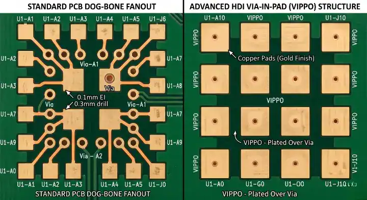
You choose dog-bone fanout for BGA pitches ≥0.8mm because standard mechanical drills fit safely between pads, but you must switch to via-in-pad (VIP) for pitches <0.65mm to prevent manufacturing clearance violations. Mastering BGA pad design and escape routing ensures you deploy the right transition at the right threshold.
Decoding Fanout Terminology
Dog-bone fanout is a traditional routing technique where a short trace (the “neck”) connects a BGA pad to an adjacent via located in the open clearance area. Via-in-Pad (VIP) is an advanced HDI technique where the via is drilled directly inside the component’s solder pad, freeing up crucial surface routing space.
Why VIPPO is Non-Negotiable
When using Via-in-Pad, you cannot leave the via hollow. VIPPO (Via-in-Pad Plated Over) requires the via to be filled with epoxy, planarized flat, and copper-plated to create a perfect soldering surface. If you use standard solder mask plugging for via-in-pad, liquid solder paste will wick down the hole during assembly, starving the joint and dropping your yield to below 70%.
Bottom line: Use cheap dog-bone fanouts whenever physics allows (≥0.8mm), but mandate epoxy-filled VIPPO the moment you drop below 0.65mm pitch.
3. What Fine-Pitch BGA Fanout Strategy Works for 0.8mm Pitch?
For an 0.8mm pitch BGA, the standard dog-bone fanout strategy works perfectly using a 6mil mechanical or laser drill with a 10mil capture pad. This geometry safely leaves enough room to route a standard 4mil trace between adjacent vias without triggering expensive HDI manufacturing tiers.
The Geometric Math
At 0.8mm (31.5mils), the distance between pad centers is substantial. If your BGA pad is 14mils, you have 17.5mils of free space between pads.
- This allows you to drop a 10mil via pad into the clearance area.
- You still have 7.5mils of remaining gap, which comfortably fits a 4mil trace with 3.5mil spacing.
Table 1: BGA Pitch Fanout Parameter Matrix
| BGA Pitch | Recommended Fanout Style | Via Type / Hole | Pad Size | Recommended Stackup |
|---|---|---|---|---|
| 0.80mm | Dog-bone | Through/Micro (6mil) | 10mil | Standard Multi-layer |
| 0.65mm | VIPPO (Optional) | Microvia (5mil) | 10mil | 1+N+1 HDI |
| 0.50mm | VIPPO (Required) | Microvia (4-5mil) | 8-10mil | 1+N+1 or 2+N+2 HDI |
| 0.40mm | VIPPO / Staggered | Laser (75µm) | 150µm | 2+N+2 HDI |
| 0.30mm | VIPPO / Stacked | Laser (75µm) | 150µm | ELIC |
Analysis Guide: Use this matrix to set your CAD constraints before routing. If your pitch is 0.4mm, immediately configure your software for 75µm laser microvias.
Bottom line: The 0.8mm pitch is the “safe zone” where standard through-hole manufacturing and dog-bone fanouts keep your PCB costs at baseline.
4. How Do You Route 0.65mm Pitch BGA Fanout on HDI PCB?
You route a 0.65mm pitch BGA by adopting a borderline strategy: use dog-bone fanouts for the outer two rows, but transition to via-in-pad with 5mil laser microvias for the deep inner pins to prevent routing congestion. This hybrid approach minimizes HDI costs while ensuring 100% escape success.
The Sub-Lamination Alternative
A 0.65mm pitch is the awkward middle ground. While you can squeeze mechanical drills in, you frequently exhaust your trace routing channels.
- Instead of jumping to a full 2+N+2 architecture, utilize a 1+N+1 stackup.
- Use blind microvias to drop signals from the surface directly to Layer 2, freeing up Layer 1 to escape route the deeper inner pins.
Pad Definition Impact
At 0.65mm, your choice between SMD (Solder Mask Defined) and NSMD (Non-Solder Mask Defined) pads becomes critical. NSMD pads provide a larger surface area for the solder ball to grip the copper sides, reducing mechanical stress. However, if space is incredibly tight, SMD pads allow for wider trace routing between components.
Bottom line: Treat 0.65mm as the transition pitch; use sub-lamination blind vias to handle inner rows without paying for extreme high-density processing.
5. What Microvia Configuration Fits 0.5mm Pitch BGA Fanout?
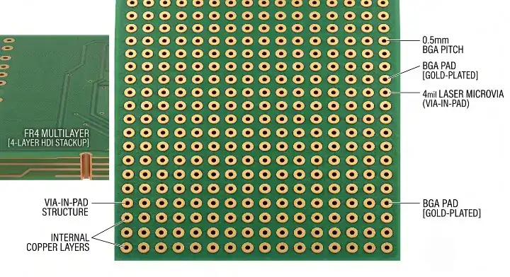
A 0.5mm pitch BGA fanout absolutely requires VIPPO technology with a 4–5mil laser-drilled microvia, an 8–10mil capture pad, and a strict 3mil annular ring. Attempting to use dog-bone routing at this density will trigger hundreds of DRC spacing errors because the vias physically overlap. Applying proper microvia optimization for HDI design resolves these geometric conflicts instantly.
Solving the EAGLE Forum Dilemma
A frustrated designer on an EAGLE forum asked: “While walking the route for a 0.5mm BGA, EAGLE does not let me place a micro-via in between the BGA pads. Is this how it is supposed to behave?”
Yes, this is exactly how CAD software should behave. At 0.5mm (19.6mils), if your BGA pad is 10mils, the gap between pads is only 9.6mils. You cannot fit a trace, a via, and safe clearances into 9.6mils. You must switch your CAD tool’s rules from standard routing to HDI rules, enabling Via-in-Pad.
The Solder Mask Dam Requirement
When setting up your 0.5mm VIPPO pads, you must enforce a minimum solder mask dam of 15µm. A solder mask dam is the thin strip of protective green resin between two adjacent surface pads. If your clearance is too tight and the manufacturer cannot print this dam, solder paste will flow between the pads, causing massive bridging shorts. Relying on a PCB annular ring design formula ensures your capture pads leave enough room for this protective dam.
Bottom line: For 0.5mm pitch and below, VIPPO is non-negotiable. Dog-bone fanout fails at this pitch regardless of how much you tweak trace widths.
6. How Do You Tackle 0.4mm Pitch Fine-Pitch BGA Fanout HDI PCB Design?
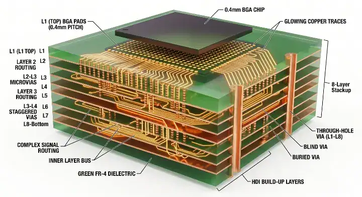
You tackle a 0.4mm pitch BGA by deploying a 2+N+2 HDI stack-up utilizing staggered 75µm (3mil) laser microvias and 150µm (6mil) capture pads. At this extreme density, you must explicitly specify IPC-4761 Type VII filled-and-capped vias in your Gerber files, or the factory will reject the design.
Confronting the FEDEVEL routing Challenge
A designer on the FEDEVEL forum posted: “I’m using a 0.35mm pitch WLP. We are trying to route it on a 6-layer board (Top/GND/Sig/Sig/GND/Bot). We have to route signals on the GND layer to fan out. Are there alternatives?”
Routing a 0.35mm/0.4mm pitch on a standard 6-layer board is a guaranteed failure. You cannot route signals across your solid GND plane without destroying your return paths and introducing massive crosstalk. You must upgrade to an 8-layer 2+N+2 HDI board. Use Layer 1 to route the outer row, use L1-L2 blind vias for the second row, and use staggered L1-L2-L3 microvias to reach dedicated inner signal layers safely.
The QueenEMS Engineering Perspective
Optimizing your Z-axis transitions saves money on extreme pitches.
- The Problem: A customer submitted a 0.4mm 484-pin BGA that required an expensive 14-layer HDI board just to complete the fanout due to massive inner row congestion.
- Our Solution: We optimized the fanout by pre-routing outer GND and Power pins directly to their respective planes using short VIPPO drops, clearing massive channels. We then allocated a strict 2 signal rows per inner layer.
- The Result: The board dropped from 14 layers down to 10 layers, fanout completion jumped from 67% to 100%, and bare board cost dropped by 25%.
Bottom line: A 0.4mm pitch component automatically dictates a minimum 8-layer 2+N+2 HDI architecture; standard through-hole boards cannot survive this density.
7. What Stack-Up Supports 0.3mm Pitch BGA Escape Routing?
A 0.3mm pitch BGA strictly requires an ELIC (Every Layer Interconnect) stack-up utilizing stacked microvias with 75µm holes and 150µm pads to complete the breakout. At 0.3mm, even staggered microvias consume too much lateral space, forcing you to stack laser drills directly on top of each other to drop signals vertically through the board.
The Stacked Microvia Risk
While stacked microvias provide maximum density, they carry inherent reliability risks. Every stacked joint adds thermomechanical stress during reflow.
- You must limit your stacks to a maximum of 2 consecutive layers whenever possible.
- If you must stack 3 layers for a 0.3mm BGA, you must demand 100% void-free copper filling verified by X-ray inspection at the factory.
Inner Row Breakout Strategy
To break out a deep 0.3mm matrix, implement this strict sequence:
- Route the outermost row directly on Layer 1.
- Drop Row 2 GND pins immediately to the Layer 2 GND plane to clear space.
- Use stacked microvias to push Row 3 and Row 4 to deeper inner signal layers.
- Push central high-speed signals to deep stripline layers with adjacent solid ground planes for perfect shielding.
Bottom line: Do not attempt a 0.3mm BGA design unless you have the budget and factory support for an ELIC stack-up with X-ray verified stacked microvias.
8. How Many Signal Layers Do You Need for Your BGA Fanout?
You calculate the required signal layers for your BGA fanout using the formula: Total inner signals ÷ (4 sides × Routing signals per channel side). For example, a dense 256-pin BGA might require 4 dedicated signal layers on an HDI board, whereas the same chip on a standard board would require 8 layers.
Table 2: Signal Layer Allocation Strategy (e.g., 0.4mm 256-pin BGA)
| BGA Matrix Rows | Escape Layer Assignment | Via Type Utilized |
|---|---|---|
| Rows 1 & 2 (Outer) | Layer 1 (Top Surface) | Surface Traces / VIPPO |
| Rows 3 & 4 (Inner) | Layer 3 (Inner Signal) | L1-L2-L3 Staggered Microvia |
| Rows 5 & 6 (Deep) | Layer 4 or 6 (Inner) | Deep Blind / Stacked Microvia |
| Center Matrix | Ground / Power Planes | Direct Via to Plane |
Analysis Guide: Never attempt to escape more than 2 BGA rows on a single inner signal layer. Overloading a layer causes unresolvable congestion.
Power and Ground First
A critical rule of fanout is to process your Power and GND pins first. By immediately dropping external and corner GND pins to the Layer 2 ground plane using VIPPO, you instantly open up wide routing channels. This allows you to route the complex, deep inner-row signal pins outward through the gaps you just created.
Bottom line: Each dedicated signal layer should escape no more than 2 BGA rows. Overloading a single layer causes routing congestion that no DRC adjustment can solve.
9. How Do You Maintain Controlled Impedance During BGA Fanout?
You maintain controlled impedance during BGA fanout by utilizing neck-down techniques, where a trace shrinks to 4mils inside the BGA coordinates to pass between pins, then expands to 5mils outside to hit the 50Ω target. As long as the neck-down length is shorter than 1/6th of the electrical wavelength, the impedance discontinuity remains well within the ±10% IPC-2221 tolerance.
The Altium Room Setup
An engineer on the edaboard forum asked: “How do I set escape routes to be 4 mil inside the package but turn into 5 mil outside while maintaining impedance in Altium?”
You achieve this by defining a specific “Room” around the BGA footprint in your CAD software.
- Set a localized Design Rule Check (DRC) for that specific room allowing 4mil trace widths.
- Keep your global board rules set to 5mils.
- When the trace crosses the boundary of the room, the software will automatically taper the trace back to the optimal impedance width.
Differential Pair Consistency
When routing differential pairs out of a fine-pitch BGA, consistency is paramount. Both traces in the pair must undergo the exact same neck-down dimension and span the exact same length before expanding. When crossing layers via microvias, always place a nearby GND stitching via to ensure the return path transitions layers identically.
Bottom line: Use neck-down traces inside the BGA array to escape tight pitches, but expand them immediately upon exiting the footprint to maintain strict impedance targets.
10. What Common BGA Fanout Mistakes Cause Manufacturing Failures?
Common BGA fanout mistakes cause 30% of HDI manufacturing failures, specifically when designers skip fanout planning, mix dog-bone and VIPPO styles under the same chip, or place dense BGAs too close to the board edge. Because sequential lamination is irreversible, these layout errors force total board scraps.
Identifying the Top 5 Fanout Mistakes
Experts across the SierraConnect and NextPCB forums repeatedly highlight these critical layout errors:
- Mistake #1: Skipping the fanout draft. Choosing an 8-layer stackup before proving the 0.4mm BGA can actually escape.
- Mistake #2: Mixing fanout styles. Using dog-bone for outer rows and VIPPO for inner rows on the same component creates uneven thermal profiles during reflow, increasing assembly risks.
- Mistake #3: Inner layer overload. Attempting to squeeze 3 or 4 rows of signals onto a single inner routing layer.
- Mistake #4: Starved GND pins. Dropping a GND pin to a plane without proper thermal relief, leading to cold solder joints or voiding.
- Mistake #5: Edge proximity. Placing a 500-pin BGA 2mm from the board edge, stripping away 25% of the available 360-degree fanout breathing room.
The QueenEMS Engineering Perspective
Proper via filling guarantees assembly yields.
- The Problem: A client experienced a 70% assembly yield on their 0.5mm BGA because they used standard solder mask to plug their via-in-pad structures, resulting in massive solder voiding.
- Our Solution: We updated their fab notes to strictly require IPC-4761 Type VII copper-filled VIPPO with planarization.
- The Result: Solder wicking was completely eliminated, and BGA assembly yields stabilized at a flawless ≥98% across mass production.
Bottom line: Never mix dog-bone and VIPPO fanout styles under the same fine-pitch component; enforce uniform pad geometries to guarantee a perfect reflow profile.
Conclusion
Executing a fine-pitch BGA fanout on an HDI PCB requires strict adherence to geometry. Whether you are using dog-bone routing for an 0.8mm component or deploying complex 2+N+2 staggered microvias for a 0.4mm processor, your layout success hinges on making the right via and pad choices before finalizing your stackup. By calculating your layer requirements early and enforcing controlled neck-down traces, you eliminate the redesign loops that plague high-density projects.
QueenEMS specializes in transforming dense schematic designs into highly reliable, manufacturable physical boards. If you are struggling to escape route a complex 0.35mm pitch BGA or need to optimize your VIPPO structures for mass production, contact our PCB layout engineering team today. We provide free front-end DFM reviews to ensure your fanout strategy is perfectly aligned with advanced manufacturing capabilities.
Written by the QueenEMS Engineering Team
FAQs
Can I use a 6-layer standard board for a 0.4mm pitch BGA? No, a 0.4mm pitch BGA requires too many fine escape channels and cannot fan out using standard through-hole vias. You must upgrade to an 8-layer 2+N+2 HDI stackup with 75µm laser microvias to successfully route the inner pins without destroying your ground planes.
What is the difference between dog-bone fanout and Via-in-Pad? Dog-bone fanout uses a short trace to connect a component pad to an adjacent via in an open area, suitable for pitches ≥0.8mm. Via-in-Pad places the via directly inside the component pad to save space, which is strictly required for pitches <0.65mm to prevent clearance violations.
Why do I need to fill Via-in-Pad (VIPPO) structures? Yes, you absolutely must fill VIPPO structures with epoxy and plate them flat. If left hollow or improperly plugged with solder mask, liquid solder paste will wick down into the hole during assembly, causing weak joints, opens, and massive yield losses.
How many signals can I route between 0.5mm BGA pads? At 0.5mm pitch, you generally cannot route any standard traces between adjacent pads on the surface layer. The physical gap is too small once you account for the pad size and manufacturing clearances, forcing you to drop signals to inner layers immediately via microvias.
Does trace neck-down ruin controlled impedance? No, trace neck-down does not significantly ruin controlled impedance if applied correctly. As long as the thinner 4mil trace inside the BGA area is shorter than 1/6th of the signal’s electrical wavelength, the brief impedance shift remains well within the acceptable ±10% tolerance margin.
Upload your files today · Free DFM check before production · Ship worldwide
Get your PCB prototypes in as fast as 24 hours. We handle FR4, Rogers, and Flex up to 60 layers — free prototypes for 2–4 layer boards, no minimum order.
Just upload your Gerber + BOM — we source every part, assemble, and inspect (AOI + X‑Ray) so you don't have to chase suppliers. Boards ship in as fast as 24 hours.