
Blog
PCB fabrication, PCB assembly, PCB materials, DFM, SMT, HDI, ceramic PCB, and electronics manufacturing guides from QueenEMS.
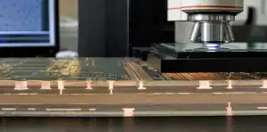
How PCB Pattern Plating Supports Reliable Trace Geometry
PCB pattern plating review connects finished trace geometry, copper profile, measurement evidence, and CAM approval before release….
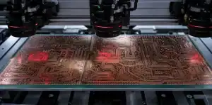
How PCB Outer-Layer AOI Can Improve PCB Quality
PCB outer-layer AOI evidence should identify the approved reference, visible circuit exception, disposition, and retention record….
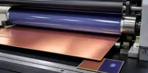
PCB Dry-Film Resist Defects: Reliable Imaging Results
PCB dry-film resist defects can change circuit geometry before imaging, plating, and etching add irreversible value….
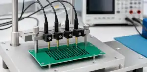
How PCB Carbon Ink Acceptance Can Improve Contact Life
PCB carbon ink acceptance should define cure, resistance, test conditions, wear, handling, and lot evidence before release….
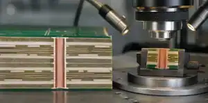
How PTH Hole-Wall Metallization Supports Reliable Vias
PTH hole-wall metallization needs named hole families, targeted evidence, and release criteria before a controlled board moves to production….
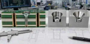
PCB Counterbore vs Countersink: 7 RFQ Rules to Know
Compare PCB counterbore vs countersink callouts with the screw geometry, controlled face, copper clearance, and first-article evidence needed before RFQ….
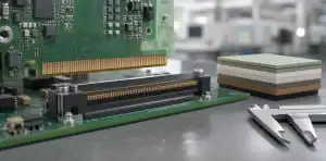
PCB Edge Connector Bevel: 5 Costly Fit Mistakes
Define a PCB edge connector bevel with the socket geometry, board face, finger finish, inner-copper clearance, and insertion evidence needed before release….
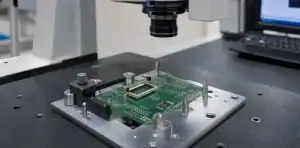
PCB Hole Position Tolerance: 5 Costly Datum Mistakes
Set PCB hole position tolerance from assembly datums, functional fit, measurement setup, and first-article evidence instead of nominal drill coordinates alone….
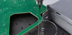
PCB Internal Corner Radius: 5 Costly Routing Mistakes
Control PCB internal corner radius with real router geometry, relief features, copper keepouts, pocket sections, and a functional fit check before fabrication….
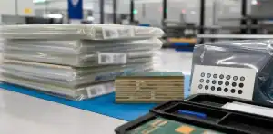
PCB Prepreg Storage Moisture Control: 5 Risky Mistakes
Manage PCB prepreg storage moisture control through material identity, lot handling, exposure disposition, stackup risk, and lamination-release evidence….
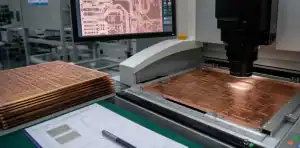
PCB Inner-Layer AOI Evidence: 5 Costly Record Mistakes
Use PCB inner-layer AOI evidence to link etched artwork, panel identity, defect disposition, record retention, and lamination release before layers are buried….
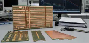
How to Specify Rogers RO1200 PCB material
Specify RO1200 laminate and bondply as a production stackup with controlled glass, copper, model values, fabrication limits, and coupon evidence….