
Blog
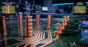
HDI Stacked vs Staggered Microvia: Which Stops BGA Failure?
Table of Contents Every month, a hardware team comes to us after their prototype failed in the field, only to discover a…
How to Choose Between Copper Fill vs Resin Fill for Via in Pad Design
Table of Contents Every week, a designer asks us why their high-density BGA board failed X-ray inspection. They thought specifying “plugged vias”…

How to Pass Ceramic PCB Thermal Cycling Tests at 150°C
Table of Contents Power module engineers often face catastrophic field failures when components crack under extreme temperature swings. This ceramic PCB thermal…
How to Prevent Ceramic PCB Warping After Eutectic Bonding
Table of Contents You can eliminate ceramic PCB warping by balancing the top and bottom copper volume ratio to exactly 0.9–1.1 and…
How to Choose DPC vs DBC Ceramic PCB
Table of Contents Choosing the wrong metallization for your high-power substrate directly results in copper delamination, routing bottlenecks, or completely blown production…
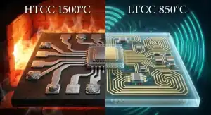
HTCC vs LTCC Ceramic PCB: How to Choose the Right Co-Fired Technology for Your Application
Table of Contents Are you specifying an expensive HTCC board for a sensor that doesn’t actually need hermetic sealing, or are you…
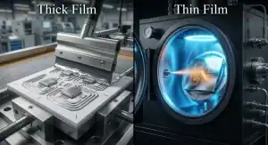
How to Choose Between Thick Film and Thin Film Ceramic PCB: A Process Decision Guide
Table of Contents Are you overpaying for ceramic manufacturing precision you don’t actually need, or are you losing high-frequency signals because your…

How to Read a Ceramic PCB Datasheet: 8 Specifications Engineers Get Wrong
Table of Contents Do your thermal simulations perfectly match your prototype boards, or do the physical chips run surprisingly hot? When engineers…

How to Qualify a Ceramic PCB for Automotive Use: AEC-Q200 and Thermal Cycling Requirements Explained
Table of Contents Are you struggling to get your new EV on-board charger substrate approved by a Tier-1 auditor? Many engineers submit…
AMB Ceramic PCB vs DBC: Which Substrate Do You Need?
Table of Contents Does your power module suffer from copper delamination after just a few hundred thermal cycles? Standard alumina substrates frequently…
How to Choose: ENIG vs Hard Gold vs Soft Gold
Table of Contents Hardware engineers frequently face costly field failures when specifying the wrong gold finish for their printed circuit boards. Choosing…
How to Design PCB Pads for Carbon Ink Printing
Table of Contents Many hardware teams face severe budget overruns when specifying hard gold for large membrane switch panels or multi-button controllers….