
Blog
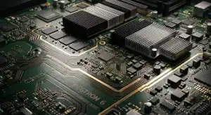
How to Spec Megtron 6 vs Tachyon 100G & M8 Upgrades
Table of Contents What Is Megtron 6 and Why Did It Define the M6 Grade Standard? Panasonic Megtron 6 (R-5775) is a…
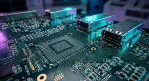
How to Spec Megtron 7 PCBs & Compare vs Tachyon 100G
Table of Contents What Is Megtron 7 and Why Is It the Bridge Between M6 and M8? Panasonic Megtron 7 (R-5785) is…
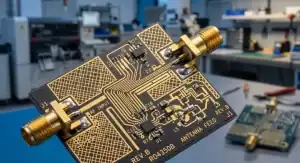
How to Avoid RO4350B Dk Traps & Compare Astra MT77
Table of Contents What Is Rogers RO4350B and Why Is It the RF Industry’s Default Laminate? Rogers RO4350B is a hydrocarbon/ceramic laminate…
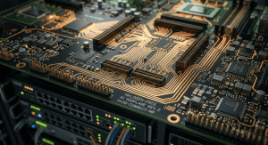
FR408HR PCB: The Hidden Hero of AI Server Hybrid Stackups
FR408HR is Isola’s high-reliability, high-performance FR-4 laminate with a Df of 0.0092 and a high Tg of 190°C (DSC). While it is…
How to Decide if I-Tera MT40 is Enough
I-Tera MT40 is Isola’s mid-loss, FR-4-process-compatible laminate with Dk 3.45 and Df 0.0031 at 10 GHz, positioned as the cost-effective sweet spot…
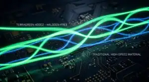
How to Use TerraGreen 400G2 for 5G and AI Server PCBs
For decades, hardware engineers accepted a painful trade-off: if your design required halogen-free environmental compliance, you had to sacrifice electrical performance. This…

How to Build Hybrid RF PCBs Using Astra MT77 Laminates
Pushing millimeter-wave designs into mass production requires balancing electrical performance with fabrication reality. This engineering Astra MT77 guide explains how to secure…

How to Beat Megtron 8 Lead Times: M8 CCL Comparison
Navigating material allocation in 2026 requires understanding the exact trade-offs between top-tier PCB laminates. This M8 CCL comparison provides a fabrication-level breakdown…
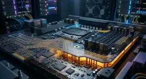
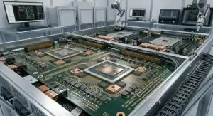
AI Accelerator PCB Material: Trainium Layer Counts
You secure a contract to manufacture a custom AI server rack for a hyperscaler, but the bill of materials does not call…
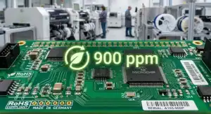
How to Specify a Halogen-Free PCB: Cost & Manufacturing Rules
You land a new contract with a European automotive tier 1, and the spec sheet clearly states: “All PCBs must comply with…
Doosan DS-7409 CCL Family: M8 and M9 Materials for AI Servers
Hardware engineers frequently face severe signal integrity bottlenecks and prolonged material allocation delays when designing 112G and 224G AI architectures. When legacy…
NVIDIA Blackwell PCB Material Guide: GB200, GB300 & Beyond
Many hardware engineering teams designing infrastructure around the latest AI platforms struggle to define the exact bare-board specifications required to survive 120…