
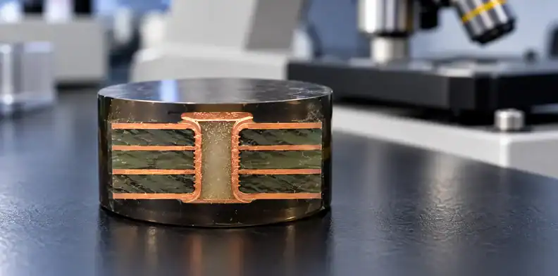
Quick Answer: Treat PCB pink ring as a reason to request evidence before deciding the affected lot. It indicates that process chemistry reached treated inner-layer copper near a drilled hole; the color alone does not establish the condition of the bond or plated barrel. Match the observed location to the inspection findings and the requirements on your order before accepting or rejecting it.
A supplier may describe a pink ring as harmless while your receiving inspector calls it delamination. Before either description becomes the shipment decision, establish what was actually observed and which requirement applies. A photograph and an unexplained “passed inspection” statement leave both questions open.
What is PCB pink ring, and where do you see it?
PCB pink ring is exposed copper coloration around a hole at an inner-layer bonding interface, where chemistry has removed some of the copper's bonding treatment. Establish the layer and viewing direction before interpreting a photograph. A mark on an accessible outer pad does not automatically identify this internal phenomenon.
In the published interlaminar bonding study, researchers exposed the relevant inner-layer area by grinding away the outer pad before microscopic examination. That preparation matters: the reported observation concerns an internal copper interface, rather than every reddish mark visible on a finished board.
Ask whether the image shows a prepared coupon, a section, an exposed inner layer, or the finished surface. Preserve that description with the image. Without it, two people can use the same defect name for different features and request the wrong follow-up inspection.
What causes pink ring after PCB drilling?
Pink ring can form when wet-process chemistry reaches treated inner-layer copper through an opening near a drilled hole. Published analyses describe drilling-related cracks and an etchback wedge at the copper-to-resin interface as possible access paths. The appearance directs attention to the manufacturing sequence, but does not identify one failed operation by itself.
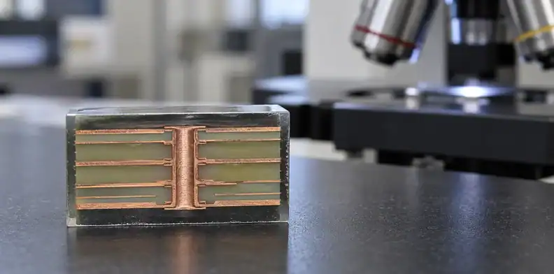
Michael Carano's technical discussion of oxide alternatives connects the observation with lamination bonding, laminate material, drilling, desmear and metallization. It describes acid entering an interface and removing part of the treated copper surface. Calling the ring ordinary surface contamination misses that mechanism.
For a supplier investigation, request the observation's position in that sequence. At which process stage was it first seen, and on what specimen? If samples are compared, were they prepared the same way? Keep treatment selection and chemistry control within the separate innerlayer oxide and lamination discussion; this decision starts with a specific observed feature.
Is pink ring a reason to reject a PCB lot?
The ring alone is insufficient grounds for a technical rejection or an unconditional acceptance. Compare the actual finding with the standard edition, product class and drawing requirements agreed for the order. If those requirements or the feature's condition remain unresolved, retain the affected material for investigation instead of guessing from its color.
Carano's 2014 column described pink ring as a process indicator under the historical IPC-600H reference it cited. That dated statement should not be substituted for the acceptance wording in your own purchase specification. It also does not establish that this shipment has no associated structural damage.
Ask the supplier to identify the requirement and explain how its evidence answers it. A customer-specific drawing restriction needs its own response. Conversely, rejecting a whole lot because a generic webpage calls every pink ring a reliability failure skips the same comparison.
What can a visible pink ring prove, and what can't it?
A correctly identified ring supports an observation about chemical access to treated copper. It cannot, by color alone, establish the extent of an opening, the integrity of the plated connection, or the cause of the condition. Evaluate each supplied result according to the property and location it actually examined.
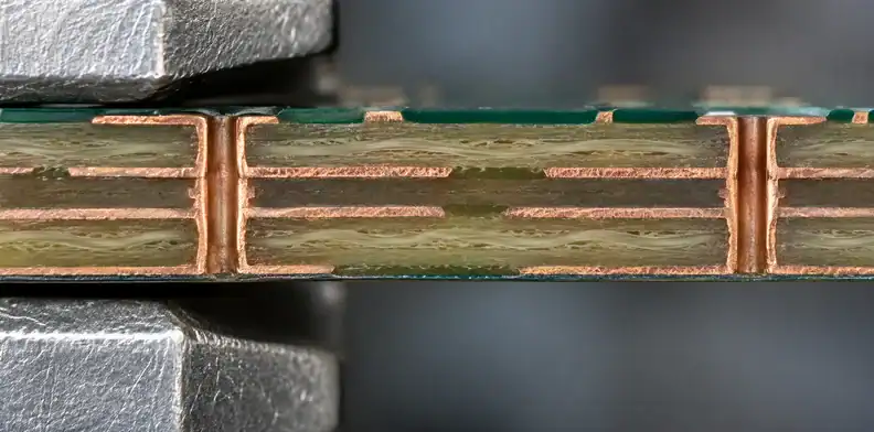
Use this buyer's matrix to keep an observation separate from the shipment decision:
| Supplier evidence | What it can support | What to request next |
|---|---|---|
| Prepared image showing pink copper around a hole | Appearance at the identified interface | Hole and layer identification, preparation method, and any associated structural finding |
| Paler ring after a bake | A change in appearance after that treatment | Treatment timing and evidence about the interface; color improvement does not demonstrate rebonding |
| Located section through an affected feature | The condition visible in that particular section | Comparison with the governing requirement and an explanation of the sampling scope |
This matrix is an editorial purchasing aid, not an IPC acceptance table.
The bonding study evaluated pink-ring resistance separately from other properties, including bond strength and thermal performance. A successful result for one property cannot establish all the others. Likewise, an electrical pass does not explain an unexamined interface: ask what the electrical test measured and keep the structural question identifiable.
Does baking remove pink ring or repair the bond?
A less visible ring after baking does not establish a repaired bond. A CALCE paper on PCB moisture control reports the belief that a post-drill bake relaxes the epoxy enough to close a crack but does not reseal it. The authors describe that bake as a cosmetic fix that also hardens epoxy smear.
This finding appears in section 4.2 of Sood and Pecht's Controlling Moisture in Printed Circuit Boards. It concerns baking after drilling in the fabrication sequence. The paper separately discusses drying boards to manage absorbed moisture before assembly; those are different process questions.
If a supplier proposes baking as its response, ask which purpose it serves and when it occurs. Do not infer that a closed-looking interface has regained its original adhesion. A drying treatment may address moisture while leaving a structural finding unresolved. This evidence does not provide a universal bake temperature or duration for your finished boards.
What should a supplier send before you decide the lot?
Request enough information to connect the photographed feature, its processing history, and the technical disposition. The response should locate the ring, explain how the observation was obtained, identify any subsequent treatment, and relate relevant inspection to the order's requirement. An unexplained “acceptable” stamp leaves the basis of acceptance unavailable to your receiving team.
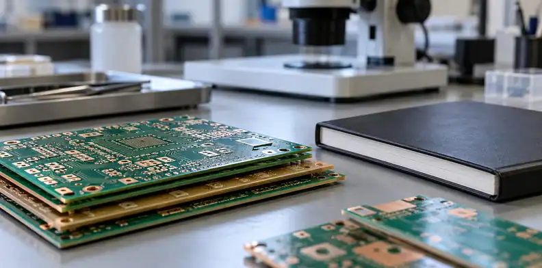
The following checklist is a buyer recommendation. It organizes the particular pink-ring question without prescribing a laboratory method or sampling plan.
| Item to obtain | What a usable response contains |
|---|---|
| Affected material and feature | Part revision, lot or panel identity, hole location and relevant layer |
| Image context | Viewing direction, specimen preparation, and whether it shows the surface or an exposed internal interface |
| Processing history | When the condition was first seen and whether the sample was baked or otherwise treated afterward |
| Inspection tied to the observation | Located findings from an affected feature, with the inspected scope and remaining limitations |
| Decision basis | Applicable order requirement, explanation of conformity or deviation, authorized approver, and material covered |
Consider a hypothetical supplier reply, written for illustration: “The ring became faint after baking, and electrical testing passed.” That reply supplies two results, but neither describes the bond at the observed interface. Ask when the bake occurred and request a located examination addressing the remaining concern. A section from an unidentified, unaffected coupon would not automatically resolve it.
For a new fabrication inquiry, submit Gerber data and the BOM for pricing and a free DFM check, with the drawing and any relevant pink-ring observations. Identify a bare-board-only request so assembly documentation is not treated as necessary; a BOM is for the assembly scope.
When should the lot stay on hold, and who decides?
Keep affected material on hold when the evidence cannot resolve the applicable requirement: the feature is unlocated, the inspection addresses a different sample, treatment history is missing, or a structural finding has no technical disposition. Assign the decision to your authorized engineering or quality function, and record precisely which material the decision covers.
Acceptance should explain why the located findings meet the order's requirements. A deviation needs authorization from whoever owns the requirement, including your own customer where their drawing or contract applies. Rejection should identify the nonconformity and affected scope, rather than depend on a color label. Where the supplier's sampling cannot justify a lot-wide conclusion, resolve that limitation before extending the decision.
For repeat manufacture, carry forward any agreed inspection or drawing change explicitly. An exception for this shipment should not quietly become permission for future lots. QueenEMS' routine board range reaches 24 layers; advanced builds can reach 100 layers, while extreme specifications can be prototyped, with volume production not guaranteed. Discuss the construction and inspection scope against the PCB capabilities before ordering.
What else do buyers ask about PCB pink ring?
Buyers also need to distinguish the internal phenomenon from surface discoloration and understand the limits of supplier qualification results. These answers address those narrower questions. A reported treatment or laboratory result applies to its stated specimens and conditions; use it to define further review rather than importing it as a universal shipment limit.
Is pink ring the same as delamination?
No. Pink ring describes the appearance associated with removal of inner-layer bonding treatment. Delamination describes separation. A chemical access path may involve an opening at an interface, but the ring's color alone does not establish the type or extent of separation in the delivered material.
Is a reddish mark on an outer pad pink ring?
Not necessarily. First establish the interface and specimen preparation. The published mechanism concerns treated inner-layer copper near a hole. Report a finished-surface stain or finish discoloration as the observed surface condition until inspection supports a more specific identification.
Can an oxide-alternative treatment prevent pink ring?
It can improve resistance under particular conditions. The published bonding study compared treatments on specified coupons and reported different pink-ring outcomes after its exposures. That supports reviewing the treatment's qualification evidence; it does not guarantee that every board made with an oxide alternative is unaffected.
Is pink-ring resistance enough to qualify a PCB supplier?
No. The bonding paper assessed it alongside other properties. Ask which construction and tests support your product's requirements. A pink-ring result alone cannot establish the supplier's performance for other materials, interconnect structures or exposures.
For a quotation that addresses this construction, upload the Gerber package and BOM to QueenEMS for a free DFM review. Include the stackup, drawing requirements and identified observations so the inquiry defines the issue to discuss. For bare PCB fabrication, send the fabrication information and mark assembly as excluded; the BOM can be omitted.
Upload your files today · Free DFM check before production · Ship worldwide
Get your PCB prototypes in as fast as 24 hours. We handle FR4, Rogers, and hybrid boards, with standard builds up to 24 layers and higher layer counts subject to engineering review — free prototypes for 2–4 layer FR-4 boards, no minimum order.
Just upload your Gerber + BOM — we source every part, assemble, and inspect (AOI + X‑Ray) so you don't have to chase suppliers. PCB assembly typically takes 5–8 working days once all components are in stock. The confirmed delivery schedule is subject to your quotation.