Quick Answer: Circuit board trace repair starts by identifying the damaged net, its electrical duty and why the copper failed. An insulated wire, shaped copper foil or conductive ink may restore an accessible surface connection, but each requires different attachment, insulation and verification. A continuity reading alone cannot establish that the repaired board is ready for service.
Circuit board trace repair can be reasonable when a localized surface conductor is damaged and the surrounding board remains usable. The difficult decision is choosing a repair that fits the circuit and enclosure without concealing unresolved damage. The decision runs from the first photograph to the evidence needed for an engineering disposition.
Table of Contents
- What must be known before a broken trace is bridged?
- Which damage changes the repair decision?
- Choose wire, copper foil or conductive ink
- Prepare sound copper without enlarging the defect
- Build a wire jumper that stays where it belongs
- When a flat copper repair is the better fit
- What conductive ink can and cannot restore
- Verify connection, isolation and operation separately
- Three repair situations with different outcomes
- Keep the repair record useful for the next decision
What must be known before a broken trace is bridged?
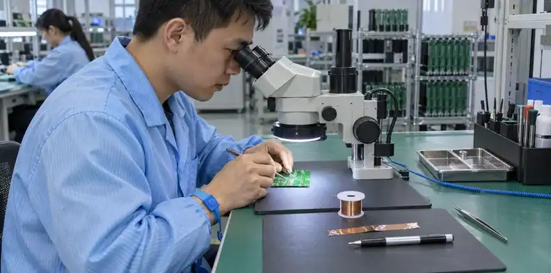
Start circuit board trace repair by establishing both endpoints, the circuit function and the damage cause before adding a conductor. Work on an isolated assembly using the product’s procedure for stored energy, then map the affected connection under magnification.
Map the net beyond the visible break
A net is the set of points that should share an electrical connection. A visible crack may sit between two pads, but the same net can also feed a via, test point or branch elsewhere. Use the schematic, artwork and a known-good assembly when available; mark which endpoints were positively identified and which remain uncertain.
The replacement route must preserve the required connections. Joining the nearest exposed copper can bypass a resistor, omit a branch or connect two separate nets. A powered-off resistance measurement helps investigate the path, although parallel components can complicate its interpretation. Record the measurement points rather than writing only “trace open.”
Separate repairable copper from unresolved damage
Look for lifted neighboring copper, a damaged via, discolored laminate and a mechanical load that could reopen the break. A scratch made during handling presents a different problem from a conductor that burned during operation. With burned copper, establish the fault before selecting a larger replacement conductor; the failed feature may have a protective role.
Use the applicable repair procedure and engineering disposition for the particular product. A published repair method does not automatically permit changes to that product. For an assembly whose thermal support also needs attention, the separate large-board rework discussion addresses that process boundary.
Which damage changes the repair decision?
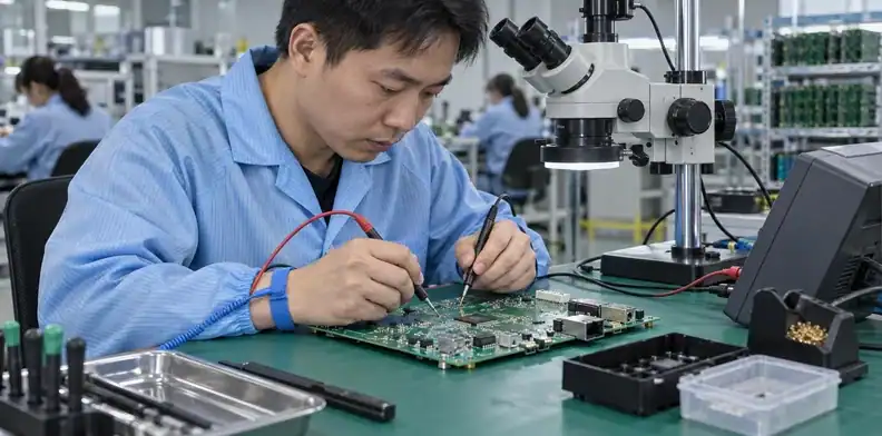
Localize the damage before deciding whether a surface conductor repair is sufficient. The table below is a screening aid for engineering review, not a blanket authorization to repair every board in a listed category.
| Observed condition | What needs checking | Possible disposition |
|---|---|---|
| Clean scratch through an accessible trace | Sound endpoints, net identity, neighboring insulation | Assess a localized conductor bridge |
| Copper lifted but still partly attached | Adhesion beyond the visible lift, pad loading | Define the damaged boundary before securing or replacing copper |
| Trace burned during operation | Fault cause, laminate condition, protection function | Hold bridging until the electrical fault is understood |
| Open connection disappears into a via | Barrel and internal-layer continuity | Escalate beyond a surface-only repair |
| Several traces damaged under a connector | Pad condition, pin mapping, connector retention | Assess a combined pad/conductor repair or replacement |
| Damage at a mating edge contact | Contact geometry, plating and wear requirements | Use a contact-specific disposition |
Photograph the defect before cleaning changes its appearance. Include an overall view to locate it and a close view with enough detail to identify nearby pins. If a connector was pulled away, retain the removed part and note the direction of force; that history can explain damage extending beneath apparently intact mask.
Edge contacts need their own treatment because a functioning bridge does not recreate the mating surface. The gold-finger repair or replacement decision covers that case. Keep the surface-trace assessment focused on the copper path that actually failed.
Choose wire, copper foil or conductive ink
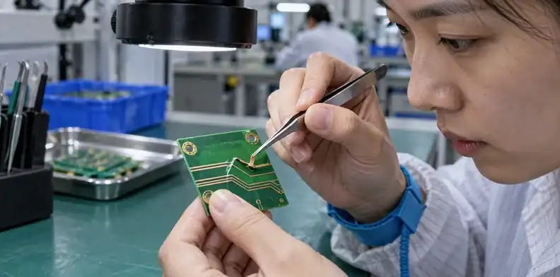
Choose the method according to electrical duty, available space and the ability to inspect and secure the result. Appearance is useful, but a flat, color-matched repair is not automatically the best conductor.
| Method | Main reason to consider it | Information needed | Limitation to resolve |
|---|---|---|---|
| Insulated wire jumper | Connects identified sound endpoints around localized damage | Current, voltage, signal behavior, endpoint geometry, route | Added height and a route that needs restraint |
| Shaped copper foil | Maintains a low-profile path over a damaged surface area | Copper thickness and width, bonding surface, overlap, clearances | Attachment and curing must suit the assembly |
| Conductive ink | Redraws a suitable low-power connection without a soldered bridge | Named product, resistance requirement, curing and coating compatibility | Product limits differ from solid copper |
Chemtronics publishes separate procedures for wire, foil and ink. Their separation is useful: these are different material systems rather than interchangeable ways to obtain the same electrical result.
Do not select a wire gauge from trace width alone. Copper thickness, duty, thermal surroundings and connection resistance also matter. The trace-width and spacing page explains the original board geometry; its design context does not automatically qualify a repair conductor.
A wire may be convenient on a slow control line yet unsuitable as an unreviewed substitute for a tightly coupled pair. Likewise, conductive ink may make a compact bridge while adding unacceptable resistance to a measurement node. Write down the property that could invalidate the chosen method before purchasing the material.
Prepare sound copper without enlarging the defect
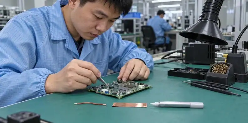
Expose only enough intact conductor for the approved attachment, and remove preparation debris before soldering or applying ink. The objective is a stable interface with known copper, not a large shiny patch.
Chemtronics’ wire-jumper procedure describes removing the damaged segment, exposing connection areas and cleaning them before attachment. Its published method is a reference for that repair system; dimensions and materials should be checked against the chosen procedure and actual board.
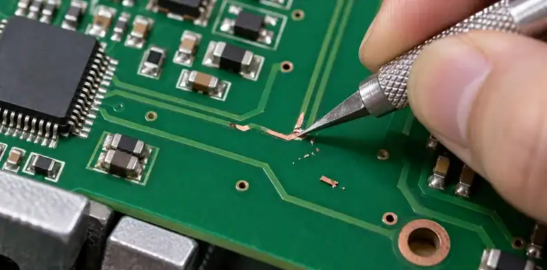
Under magnification, separate the damaged segment before lifting it away. Pulling on partly attached copper can extend the defect toward a pad. Remove mask gradually with a controlled tool, checking that the underlying conductor is not being thinned or cut. Pause if the copper moves, the attachment area disappears into a damaged pad or the laminate surface cannot support the proposed repair.
Use a cleaning agent compatible with the assembly and the repair material. Keep loosened mask particles and metallic debris away from adjacent pads. Existing solder-wick practices can help when excess solder obstructs an attachment, but braid pressure and heat must not become another source of lifted copper.
Before moving on, inspect the prepared endpoints, verify their identity again and compare the exposed area with the planned joint. A repair should not depend on copper that was assumed sound because it remained hidden beneath mask. Preserve an intermediate photograph while those interfaces are still visible.
Build a wire jumper that stays where it belongs
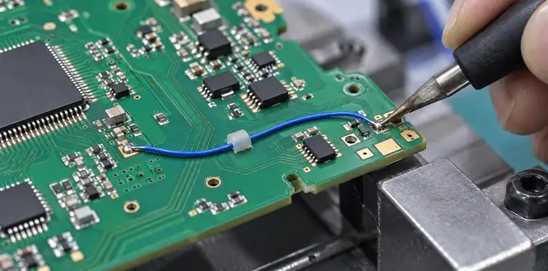
A wire jumper needs suitable electrical properties, sound terminations and mechanical restraint. Plan all three before soldering either end, especially when the route passes close to a connector or enclosure wall.
Select the conductor and attachment points
Confirm that the wire and its insulation suit the circuit’s operating conditions. Current-carrying paths need a justified conductor choice; sensitive signal paths need review of the route as well. This article supplies no universal trace-to-wire conversion because the original trace and replacement wire operate in different physical surroundings.
Choose endpoints that can accept the joint without relying on loose copper. Sometimes a documented test pad or component termination offers a more sound interface than the edges of a scratch. That alternative changes the route and may skip an intermediate branch, so it needs a net-level check. If the damaged path feeds several loads, consult the broader power-distribution considerations before assuming two visible endpoints tell the whole story.
Route and secure the wire before final inspection
Keep the wire clear of moving hardware, sharp edges, probe access and areas that will receive later soldering. Avoid leaving a taut span that transfers movement into a tiny copper attachment. Conversely, unnecessary slack can reach adjacent circuitry or become trapped during assembly.
Chemtronics’ wire method includes securing the jumper and restoring protection after soldering. Select the restraint and coating through the applicable material instructions. The repair should remain inspectable long enough to check both joints and surrounding clearances before those features are covered. A successful electrical connection still needs a route that the finished product can accommodate.
When a flat copper repair is the better fit
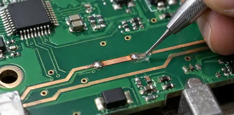
Consider shaped foil when a low-profile conductor is necessary and the surface can support a controlled bonded repair. It is particularly worth assessing where a round wire would interfere with assembly, although foil does not automatically reproduce the original electrical geometry.
The Chemtronics foil-jumper method calls for foil selected to match the conductor’s width and thickness, prepared attachment ends and an epoxy overcoat. That sequence makes the metal interface and the supporting material separate process decisions.
| Foil-repair feature | Question to answer | Evidence to retain |
|---|---|---|
| Replacement copper | Is its cross-section appropriate for this circuit? | Material identity and approved dimensions |
| Attachment overlap | Does the chosen method fit sound copper at both ends? | Photograph before covering |
| Side clearance | Can foil or solder spread approach another net? | Magnified view and relevant measurement |
| Supporting surface | Is it sound enough for the bonding system? | Damage disposition and preparation record |
| Epoxy or overcoat | Will its cure suit nearby components and later processing? | Product instructions and actual cure record |
Fit the shape before committing to solder or adhesive. Check the foil in relation to nearby holes, connector feet and housing surfaces, not only the broken path. A carefully cut conductor can still fail the assembly fit if its attachment builds excessive height.
Do not treat a green overcoat as proof that the copper is restored. Its role must be specified separately from the conductor’s role. For boards already protected by a coating system, review conformal-coating choices so the local restoration does not quietly change the intended protection.
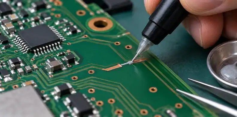
What conductive ink can and cannot restore
Conductive ink is a product-specific option for suitable low-power connections, not a general substitute for copper or a high-current jumper. Confirm the required resistance, environment and subsequent processing against the exact material.
The CircuitWorks conductive-pen product information distinguishes silver and nickel formulations and discusses low-voltage applications. Chemtronics also cautions against using its pens for high-power or high-frequency circuitry. Those limits belong to the cited products; they should not be turned into a numerical rating for an unnamed repair pen.
Application and curing are separate tasks. In its conductive-ink repair instructions, Chemtronics specifies at least one hour before overcoating. A film that looks dry may not yet meet the next process requirement. Follow the named material’s instructions for thickness, curing and compatibility instead of transferring a drying time from a forum demonstration.
On a precision sensing node, even modest added resistance can change the result; investigate the circuit’s allowable error before deciding that a meter reading is satisfactory. Ink also needs a stable supporting surface. It cannot restore a torn pad’s ability to withstand connector force simply by making the region conductive.
Keep the dispensed material away from adjacent nets and allow access for measurement before protective coating. Record the product and cure conditions so a later intermittent fault can be investigated. If those details are unknown, the repaired path has an undefined material history rather than a reproducible process.
Verify connection, isolation and operation separately
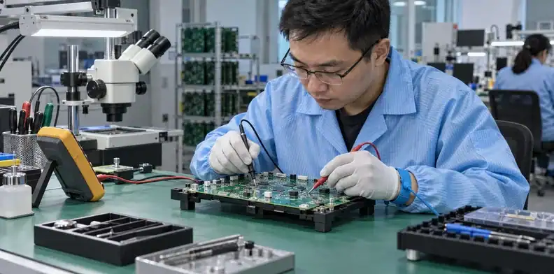
Verification should establish the correct connection, separation from other nets and intended circuit behavior. These are different questions, so a single continuity beep cannot close all of them.
Unpowered measurements come first
Inspect the route and attachments before measuring. Check for disturbed components, loose strands, conductive debris and material that obscures the interface. Then measure the designated endpoints and investigate unexpected readings using the schematic. Parallel paths can produce continuity even when the intended repair remains defective.
| Verification level | Question answered | Example record | What it does not establish |
|---|---|---|---|
| Visual and geometric | Is the repair physically acceptable for the approved method? | Joint, restraint and adjacent-clearance photographs | Electrical function |
| Connection measurement | Are the specified endpoints connected as intended? | Points, instrument and recorded result | Load behavior or insulation suitability |
| Adjacent-net isolation | Has an unintended path been introduced? | Defined net pairs and appropriate test result | Every internal-layer condition |
| Functional test | Does the affected circuit meet its requirement? | Test setup, operating condition and acceptance result | Unspecified future environments |
Functional evidence closes the repair
Apply power only after the product’s release conditions permit it, using an appropriate controlled test setup. Test the affected function rather than relying on the fact that an indicator illuminates. A repaired communication path needs relevant communication evidence; a power path needs evidence under its specified operating conditions.
Specify what a failed test will trigger before running it. The outcome may be another investigation, an alternative repair or replacement. A useful failure-analysis report connects the observed failure, corrective action and confirming evidence so that a second technician can follow the disposition.
Three repair situations with different outcomes
The same visible break can lead to different decisions when electrical duty or packaging changes. The following situations are illustrative engineering examples, not reports of repairs performed by QueenEMS.
| Situation | Decision driver | Reasonable next action | Evidence that closes the question |
|---|---|---|---|
| A tool scratches a slow control trace on a prototype | Local damage, accessible sound endpoints | Assess a restrained insulated jumper | Net identity, joints, isolation and control-function test |
| A flat assembly must slide beneath a close-fitting cover | Height and mechanical contact | Evaluate a shaped foil repair and its bonded profile | Fit inspection plus electrical verification |
| A battery-path trace opens after a fault | Cause and protective behavior | Investigate before proposing any bridge | Fault diagnosis and authorized circuit disposition |
In the prototype example, a photograph alone does not reveal whether the path is a slow control line or a clock. The schematic supplies the missing context. A repair owner can then select a method for the actual duty and document why it was accepted for that engineering unit.
For the close-fitting assembly, a wire that works on an open bench may be pressed against the cover in the product. The packaging constraint makes the foil option worth investigating, but its cure and attachment still need approval. Installation clearance becomes part of verification rather than an afterthought.
The battery example cannot be settled by installing thicker copper. That may change the fault outcome while leaving the original cause in place. The useful lesson across these examples is to identify the condition that controls the disposition: signal behavior, physical space or fault function. It gives the repair review a specific unresolved question to close.
Keep the repair record useful for the next decision
Retain enough information to reconstruct what failed, what was changed and what evidence supported the disposition. A brief record with identified measurement points is more useful than an unexplained “repair passed” stamp.
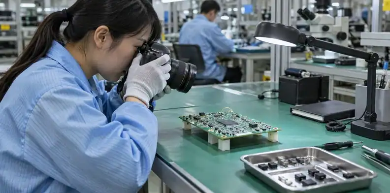
Include the board revision, assembly identifier, defect location, affected net and known failure history. Record the chosen method, wire or foil dimensions when relevant, material identities and cure conditions. Keep before, intermediate and finished photographs together so covered attachment points can still be reviewed.
The test record should name its acceptance basis and any limitation. A prototype authorized for bench evaluation is not automatically approved for shipment. If the repair required an engineering concession, preserve that decision with the unit; do not let it disappear when the board returns to assembly.
When recurring damage points to a process problem, examine the handling or soldering operation that produced it. The flux-selection discussion can support a process review where wetting and cleaning contributed, while a pulled connector calls for a mechanical investigation. Repeating the conductor repair without correcting its cause leaves the same exposure in place.
Replacement may be preferable when the structure cannot be inspected, the required function cannot be verified or the approved repair would obstruct assembly. For a replacement-board or revised-assembly inquiry, contact QueenEMS with the released fabrication data, bill of materials, damage photographs and the documented disposition so the manufacturing request starts from the actual failure.
FAQ
Can a solder blob replace the missing copper?
It should not be the default method. The bridge needs a defined conductor, suitable attachment and mechanical support. Decide whether the chosen procedure permits a soldered bridge for that particular gap and circuit.
Does conductive adhesive replace a torn connector pad?
Electrical conductivity does not establish pad retention. A torn pad introduces a mechanical attachment problem that needs a pad-specific repair disposition or replacement.
Can an internal-layer open be repaired from the surface?
A documented alternate connection may be possible in some products, but identifying the damaged internal structure and all affected branches requires engineering review. A surface bridge does not prove the hidden damage is harmless.
How much should a trace repair cost?
Cost depends on diagnosis, access, materials, inspection and the tests required for acceptance. Compare that complete scope with the cost and availability of a replacement assembly; an unsupported universal price would obscure the main decision.
Sources
- Chemtronics: wire-jumper repair method, with foil, ink and product-specific instructions cited alongside the relevant discussion.
Written by the QueenEMS Engineering Team
Upload your files today · Free DFM check before production · Ship worldwide
Get your PCB prototypes in as fast as 24 hours. We handle FR4, Rogers, and hybrid boards up to 40 layers in volume production, with advanced builds subject to engineering review — free prototypes for 2–4 layer FR-4 boards, no minimum order.
Just upload your Gerber + BOM — we source every part, assemble, and inspect (AOI + X‑Ray) so you don't have to chase suppliers. Boards ship in as fast as 24 hours.