
Quick Answer: No single test proves that a discrete chip or die embedded inside a PCB is correctly placed, connected and working after lamination. Buyers get defensible coverage by combining project-specific evidence: X-ray images of the device area, electrical tests on nets that remain reachable, and cross-sections on agreed samples. Before order release, they also fix in writing what each method cannot see and who decides acceptance for any device no test can reach.
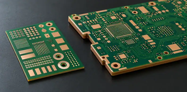
Illustrative image: an unpopulated PCB and test coupon on a bench.
Embedded discrete PCB inspection has to be planned before a component disappears beneath copper and dielectric. The order needs more than a note asking for “X-ray inspection”: it needs a way to connect each device and net to a result, a report and a decision. This guide addresses physical chips and die placed inside a board; films formed into resistors or capacitors follow a different discussion.
What Counts as an Embedded Discrete Device, and What Doesn’t?
A placed embedded device is a physical passive chip or semiconductor die incorporated into the board construction. It has an identity, location and electrical connections that must be accounted for. A resistor or capacitor formed from material within the stack is a different construction, with a different evidence plan.
The IPC-hosted paper on embedded components describes both placed passive devices and active die, along with several construction routes. Use the actual stackup and device list to establish where inspection is possible. A pre-encapsulation photo, for example, is useful only if the agreed route permits that view and the record identifies the relevant device.
For formed films and their design tradeoffs, see formed embedded passives in HDI designs. For a proposed placed-device project, ask the embedded components PCB service to confirm the specific construction and test plan. General service descriptions do not establish feasibility for your design.
What Can Embedded Discrete PCB Inspection Methods Show or Miss?
X-ray can image hidden structures without cutting the board, while an electrical test can assess only what its accessible connections and test program reach. A cross-section exposes the internal structure of the specimen that is cut. Each method answers a different question, and none alone proves function or long-term reliability.
X-ray: Ask for views of the device and its interconnections, identified by board, layer and reference designator. A view may show presence or position if the device features have enough contrast and are not obscured by overlapping structures. It may not identify the loaded part value or resolve a particular interface. Agree the usable view and interpretation criteria for the construction before relying on the image.
Electrical testing: Flying probe or ICT may reach a buried device through accessible nets, depending on the circuit and test design. A continuity result does not automatically measure a component value or demonstrate device function. Parallel paths and inaccessible nodes can also limit what a reading establishes. Ask for the test points, measured property and coverage gaps, not a generic “pass” alone.
Cross-section: A section can expose a selected internal region for direct observation, but it consumes the specimen and reveals only the plane examined. Oneida Research Services describes X-ray and cross-section inspection methods; agree which region will be sectioned and how the sample relates to the lot. A clean section does not establish that every device in every board has the same result.
How Do You Map Each Buried-Device Defect to Evidence?
Start with the question you need answered, then identify a suitable method, its limitations and the evidence your team will receive. Record the stage and decision owner alongside each item. The matrix below is a hypothetical buyer planning tool; the applicable tests and acceptance criteria must be agreed for the actual construction.
| Question or concern | Possible method and stage | Limit and evidence to request | Example decision owner |
|---|---|---|---|
| Was the correct part loaded? | Placement and material record before encapsulation, where the route allows; X-ray after lamination may show presence. | An image may not identify value or part number. Request the device-to-material-lot record. | Buyer engineering confirms the part; supplier supplies the record. |
| Is a device shifted or rotated? | X-ray after lamination if its features are distinguishable. | Overlapping copper or poor contrast can obscure orientation. Request labeled views and the agreed interpretation. | Buyer quality and supplier agree the disposition. |
| Is an internal connection open? | Electrical test on reachable nets; section a chosen sample if agreed. | An unexposed node may be untestable; a section covers only its plane. Request net coverage and sample identity. | Buyer engineering owns access; supplier reports results. |
| Has a chip cracked or changed value? | Electrical measurement where the circuit permits; section a selected sample if agreed. | An intermittent fault can pass a static measurement. Request the measured property, access and conditions. | Buyer engineering decides whether coverage is adequate. |
| Does a buried active die work? | Functional test when the design, access and assembly scope permit. | A board-level failure may not isolate the cause to the die. Request the test specification and coverage limits. | Buyer test engineering approves the functional test. |
These owner assignments are examples. Put the actual names or roles in the purchase package, including who can accept an unresolved condition. An image, a measurement and a decision can belong to different people.
Planning a board with buried devices? Upload your Gerber files, stackup and device list through our contact page for a quote and free DFM check. Include the BOM if assembly is in scope; we will review whether the proposed inspection plan is feasible for your construction.
Who Decides Acceptance When a Buried Device Cannot Be Tested?
The buyer owns acceptance of residual risk for a device no test can reach; the supplier reports evidence but cannot accept design risk on the buyer’s behalf. Before order release, the buyer can redesign for access, agree a sampling plan for the construction, or explicitly accept the remaining risk.
Start with the netlist and mark the devices and nets that have no practical access. A test point may make a measurement possible, but its location, circuit loading and production use need engineering approval. A coupon or sacrificial board can help examine a selected construction when its relationship to the production lot is agreed; it does not automatically prove every board.
If access cannot be added, describe the unresolved question in the order documentation. State what evidence will be delivered, who reviews it, and whether a missing or ambiguous result stops the lot. A supplier can explain the proposed inspection and report its results; the buyer must approve any residual design risk and the acceptance basis.
What Should Your RFQ Fix Before Order Release?
An RFQ should identify each buried device, its construction and the evidence needed to make a release decision. Include accessible nets, proposed inspection stages, a sampling plan, report format and the person who resolves coverage gaps. Have the supplier confirm feasibility for that particular board before the order is accepted.
Use this checklist as a starting point and adapt it with the fabricator and your engineering team:
- Identify: Provide Gerbers, stackup, device reference designators, part numbers, locations and the intended construction. Specify the material or part traceability you need.
- Access: Flag the reachable and unreachable nets in the netlist. Identify proposed test points or representative coupons and any circuit conditions needed for measurement.
- Stages: Agree whether a placement record is available before encapsulation, which X-ray views are useful afterward, and what electrical or functional tests apply.
- Sampling: Define the specimen, location and lot relationship for any destructive cross-section. Agree the sampling plan instead of assuming one section represents all boards.
- Decisions: State the drawing or agreed specification that supplies acceptance criteria, who owns each unresolved result, and what holds or releases a lot. Request traceable reports with board and device identifiers.
QueenEMS has more than ten years of experience and lists AOI, X-ray, flying probe, ICT and functional testing among its available test categories. AOI applies to visible surfaces, such as a pre-encapsulation view where the route provides one. Whether a method can cover a particular buried device depends on the project, test access and agreed scope. For assembly, include the BOM and assembly drawing, and clarify whether components will be supplied by the customer or sourced under a turnkey arrangement.
Frequently Asked Questions
Can X-ray alone prove an embedded device works?
No. X-ray may show a device or structural feature when the materials, geometry and image resolution permit it, but it does not demonstrate that the circuit performs its intended function. Agree which view is useful and pair it with an electrical or functional test where the design provides access.
Can in-circuit or flying-probe testing reach a buried device?
Only when the relevant connections can be reached through accessible points and the circuit allows a meaningful measurement. A probe does not touch the buried part directly. Ask for a coverage list that identifies untested nets, parallel paths and any limitations in the test program.
Does a passing cross-section qualify every production board?
No. A cross-section shows the selected plane in the specimen that was cut. Whether that specimen is useful evidence for a production lot depends on the agreed construction, sampling plan and traceability. Define the inspection location and decision criteria before destructive testing starts.
What should be fixed before order release?
Agree the device list, test access, intended evidence, sampling and report format before release. Name the person responsible for acceptance when a device or connection remains untestable. The drawing and purchase documents should identify the applicable criteria and how an unclear result will be handled.
Written by the QueenEMS Engineering Team.
Ready to request a quote? Upload your Gerber files and test coverage plan through the contact page for a free DFM check. Add your BOM if you also need assembly; the team can review the construction and identify which available tests could apply.
Upload your files today · Free DFM check before production · Ship worldwide
Get your PCB prototypes in as fast as 24 hours. We handle FR4, Rogers, and hybrid boards, with standard builds up to 24 layers and higher layer counts subject to engineering review — free prototypes for 2–4 layer FR-4 boards, no minimum order.
Just upload your Gerber + BOM — we source every part, assemble, and inspect (AOI + X‑Ray) so you don't have to chase suppliers. PCB assembly typically takes 5–8 working days once all components are in stock. The confirmed delivery schedule is subject to your quotation.