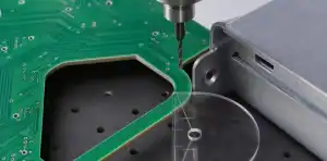
Compare PCB counterbore vs countersink callouts with the screw geometry, controlled face, copper clearance, and first-article evidence needed before RFQ.
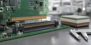
Define a PCB edge connector bevel with the socket geometry, board face, finger finish, inner-copper clearance, and insertion evidence needed before release.
Set PCB hole position tolerance from assembly datums, functional fit, measurement setup, and first-article evidence instead of nominal drill coordinates alone.
Control PCB internal corner radius with real router geometry, relief features, copper keepouts, pocket sections, and a functional fit check before fabrication.
Manage PCB prepreg storage moisture control through material identity, lot handling, exposure disposition, stackup risk, and lamination-release evidence.
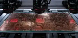
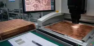
Use PCB inner-layer AOI evidence to link etched artwork, panel identity, defect disposition, record retention, and lamination release before layers are buried.