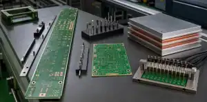
Blog Maximum PCB Size Depends on the Process Route Maximum PCB size is controlled by the smallest usable operation in the manufacturing and assembly route—not laminate sheet size alone. August 28, 2026 Read More
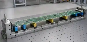
Blog Large PCB Warpage Control: How to Prevent Bow and Twist Large-board flatness is designed into the stack-up, copper distribution, mechanical system and acceptance method before fabrication begins. August 28, 2026 Read More
Blog One Large PCB vs Multiple Boards: What Should You Quote? Bare-board area is only one cost: connectors, test, repair exposure, supplier choice and revision cadence can reverse the result. August 28, 2026 Read More
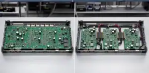
Blog Large Format PCB Assembly Across the Full SMT Line A fabricable oversized board is not automatically assemblable; every machine, transfer, support and inspection step needs a route disposition. August 28, 2026 Read More
Blog Large PCB Design Rules: How to Prevent Costly Rework Ordinary clearance checks are not enough when a large outline magnifies registration, support, copper-balance and tolerance-chain risks. August 28, 2026 Read More
Blog PCB Glass Weave Skew: 5 Costly Timing Mistakes PCB glass weave skew needs a named stack-up, routing review, and release evidence when differential-pair timing margin is tight. August 27, 2026 Read More
Blog PCB Dk and Df Test Methods: What Buyers Must Compare PCB Dk and Df test methods must be matched by frequency, construction, and stack-up before a high-speed material is approved. August 27, 2026 Read More
Blog Core vs Prepreg in PCBs: Differences and Stackup Choices Core vs prepreg construction changes impedance through resin content, press-out, copper distribution, and finished dielectric geometry. August 27, 2026 Read More
Blog 7 PCB Z-Axis CTE Checks for Better Via Reliability PCB Z-axis CTE affects via reliability through the finished stack-up, via construction, copper schedule, and qualified thermal exposure. August 27, 2026 Read More
Blog HDI Registration: 5 Costly Microvia Pad Mistakes HDI registration protects microvia landing pads by defining the buildup, target pad, margin, and CAM review before release. August 27, 2026 Read More
Blog Ceramic PCB Dielectric Strength: 5 Costly Isolation Mistakes Ceramic PCB dielectric strength must be reviewed with substrate thickness, copper geometry, isolation paths, and the defined power-module test. August 27, 2026 Read More
Blog How Multilayer PCB Resin Flow Supports Reliable Lamination Multilayer PCB resin flow review prevents starvation, squeeze-out, and unapproved stack-up changes during lamination. August 26, 2026 Read More