
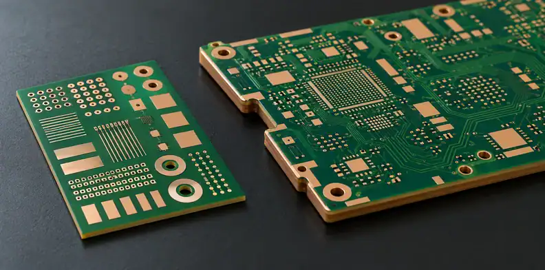
Quick Answer: A heavy copper PCB resistance test becomes an acceptance requirement when the drawing identifies the power path, force and sense points, resistance limit and temperature basis. Use separate current and voltage connections, account for thermoelectric offsets and self-heating, and report repeatability and measurement uncertainty. Agree the decision rule for near-limit results before testing; a low reading alone cannot establish copper thickness or current rating.
A supplier's “electrical test passed” report may answer a connectivity question while leaving your milliohm limit unmeasured. Start by defining the quantity you need. The receiving team and the supplier must be able to connect the same points, under the same stated conditions, and interpret the result using the same rule.
What should a heavy copper PCB resistance test prove?
A heavy copper PCB resistance test should establish the DC resistance of one identified finished-board path, at stated conditions, against a specified limit. That requires more information than a net name and a pass stamp. The requirement must distinguish an absolute resistance measurement from continuity coverage, copper-thickness inspection and design current or temperature-rise calculations.
A PCB electrical-test requirement addresses connectivity and its agreed coverage. A path-resistance requirement adds a defined measured quantity and conditions. Keep those order requirements separate so a routine open/short report is not accepted as a milliohm measurement.
Use the heavy-copper design discussion for geometry and current-sizing questions. Resistance depends on the sensed path's geometry and temperature; it cannot uniquely identify copper thickness or validate the board's operating environment. This article concerns the absolute DC reading used for acceptance, rather than resistance change during thermal cycling.
Where does the measured path begin and end?
The voltage-sense contact locations define the measured region, while the force contacts establish how current enters and leaves it. Mark both pairs on a drawing. Identify included pads, vias and plane necks, and specify the circuit state and parallel paths so a repeated measurement represents the same physical object.
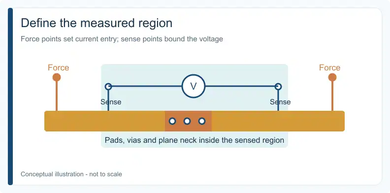
Use this suggested engineering/procurement aid as a measured-path boundary record. Its conceptual order is force contact → sense contact → defined copper/via region → sense contact → force contact. For a real plane or branched network, replace that simplified order with actual contact coordinates and current-entry geometry.
| Boundary item | Record on the drawing or fixture sheet |
|---|---|
| Path identity | Net, endpoints, board revision and path identifier |
| Force contacts | Current entry/exit locations and contact arrangement |
| Sense contacts | Voltage-pickup locations tied to drawing features |
| Included region | Pads, plane necks, vias and plated holes within the voltage boundary |
| Circuit state | Bare-board state and treatment of parallel conductive paths |
| Reproduction reference | Fixture revision and contact-placement method |
Moving a sense contact across a pad or via changes the included region. Changing the force arrangement can also change current distribution in a broad plane. A description such as “measure between the connectors” leaves too much room for two teams to measure different paths.
How do separate force and sense connections work?
A four-terminal measurement supplies current through one contact pair and senses voltage through another. This minimizes lead and contact-drop contributions outside the voltage boundary. Conductive features inside that boundary remain part of the result. Four wires therefore help isolate the intended quantity, but they do not remove every contact or geometry effect.
The Keithley low-resistance white paper, published in 2010, explains the enduring force/sense principle and error mechanisms. Its instrument examples are not PCB settings. The AEMC Kelvin connection note likewise distinguishes separate current and potential connections.
Place the sensing contacts on the intended board features rather than treating the cable connection as the measurement boundary. On a bare board, every pad, via and copper feature between the sense contacts belongs to the result, so state the board condition on the requirement. A limit intended for an assembled board would need its own boundary definition. Also examine unstable or non-ohmic contacts before treating an erratic reading as a board defect.
Which temperature belongs with the resistance limit?
The limit needs a stated reference temperature, and the reading needs a recorded DUT temperature or an agreed condition window. If correction is required, name the coefficient, source and correction method in the requirement. Comparing results taken at different, unrecorded temperatures can confuse a temperature effect with a construction difference.
The temperature-compensation explanation discusses winding and busbar measurements. The transferable principle is that resistance changes with conductor temperature; its equipment features and settings are not requirements for a PCB test.
Record how the board temperature is determined and when the reading is taken relative to conditioning and current application. Room temperature alone may not represent the current-carrying region. No numerical copper correction coefficient is prescribed here: use a sourced value applicable to the material and reference condition when your agreed method requires one.
How do thermal offsets and self-heating affect readings?
Thermoelectric voltages can add an offset to the small voltage being measured. Equal and opposite test currents allow that offset to cancel if it remains stable during the reading pair. Increasing current improves the resistive signal, but can heat the path and change its resistance, so the current and timing need control.
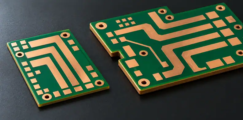
For the stable-offset case, the white paper gives R = (V₊ − V₋)/(2I). R is resistance in ohms, I is the positive current magnitude in amperes, and V₊ and V₋ are signed voltage readings in volts at equal positive and negative currents. Keep the voltage-sense polarity fixed during reversal.
Constructed arithmetic example: at I = 0.010 A, readings of +22 µV and −18 µV give R = 40 µV / 0.020 A = 0.002 Ω. The assumed common offset is +2 µV. These invented inputs demonstrate the calculation; they are not a board result, acceptance limit or test-current recommendation.
If the offset drifts during the pair, simple reversal loses that cancellation assumption. The source also describes a three-reading delta method for linear drift. Select an appropriate measurement method and check current-induced drift rather than automatically choosing the highest available current.
For a quotation and free DFM review, provide Gerber files and the fabrication drawing with the stackup and the defined path-resistance requirement. Add a BOM only if assembly is also requested. Ask for a feasibility and scope review of the specified measurement before release, since whether it can be included is confirmed per project.
Why record repeatability and measurement uncertainty?
Repeat readings show how results vary under the repeated conditions, while measurement uncertainty expresses the stated doubt associated with a result. The product tolerance defines the allowed resistance. Record these separately so an instrument display, a repeatability range and a drawing limit are not treated as interchangeable evidence when a reading approaches acceptance.
Tektronix's tolerance and uncertainty explanation separates those concepts. Repeatability alone is not the complete uncertainty statement: stable repeated readings can still share an offset or temperature error.
The record should identify the instrument, range, calibration reference, measurement method, repeat sequence and uncertainty statement applicable to the setup. Note changed contact placement or temperature rather than merging those readings into an unexplained average. Ask what the quoted uncertainty includes and how it is expressed before applying it to a decision rule.
When can a near-limit result release the lot?
A near-limit result can support release only through the decision rule agreed for that order. Define the tested population, resistance limit, temperature basis and treatment of uncertainty before measurement. Name who resolves ambiguous results, and distinguish a measured board from a coupon or sample so one passing record is not silently extended to the lot.
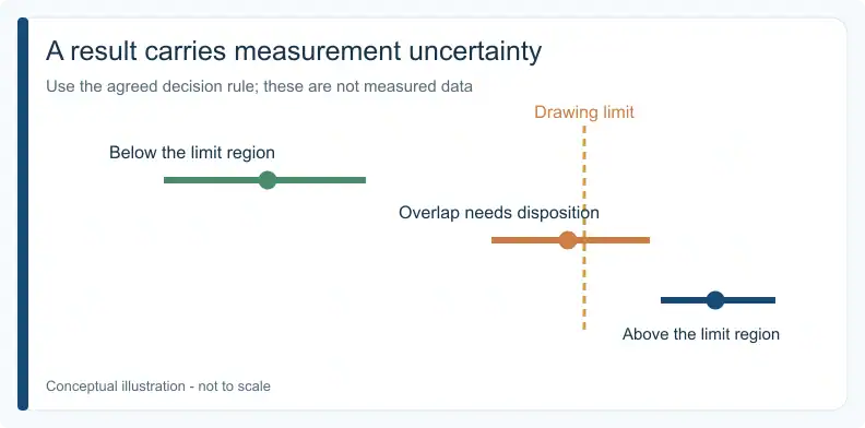
The following low-ohm acceptance worksheet is a suggested engineering/procurement aid. Complete its blank fields using the drawing and agreed test method. It supplies no universal resistance limit, sampling plan or guard band.
| Worksheet field | Required entry |
|---|---|
| Measured object | Path ID, board/coupon identity, drawing and fixture revisions |
| Acceptance requirement | Drawing limit and reference temperature |
| Applied current | Magnitude, range and reading timing |
| Voltage/result | Signed V₊, V₋, calculated R and units |
| Temperature | DUT value, agreed window or sourced correction method |
| Repeats | Sequence, count and spread |
| Measurement confidence | Instrument, calibration reference and stated uncertainty |
| Decision | Agreed rule, pass/fail/escalate outcome and authorized disposition |
When the uncertainty interval overlaps the limit, follow the negotiated rule. Adding uncertainty to the maximum allowed resistance automatically would change the acceptance requirement. Keep unresolved results on hold for the authorized disposition rather than inventing a rule after seeing the data.
Frequently Asked Questions
Why does measured path resistance differ from a calculation?
The calculation and measurement may use different boundaries, temperatures or geometry. Lead and contact contributions can also enter a two-terminal reading. Compare the sensed region and finished-board state with the model before treating the discrepancy as proof of incorrect copper thickness.
Can a low reading confirm copper thickness or current rating?
No. Resistance combines path length, cross-section, vias, parallel paths and temperature. Different constructions can yield a similar value. Current rating also depends on the board's thermal conditions and operating environment, so it needs a separate design assessment.
Should every reading use a standard copper temperature correction?
No. Apply correction only through an agreed method with a named coefficient, source, reference condition and measured DUT temperature. Otherwise, measure within an agreed temperature window. An uncited coefficient and an assumed ambient temperature do not make results comparable.
Does a result at the limit plus uncertainty automatically pass?
No. The agreed decision rule controls the outcome, including how uncertainty is treated. Product tolerance and measurement uncertainty describe different things. Record the rule before testing and refer an ambiguous result to the named disposition authority.
QueenEMS has more than 10 years of experience. For a quotation and free DFM review, submit the Gerber package and stackup with the marked measurement boundary and acceptance requirement. Add a BOM if assembly is requested, and resolve the required evidence scope before releasing the order.
Upload your files today · Free DFM check before production · Ship worldwide
Get your PCB prototypes in as fast as 24 hours. We handle FR4, Rogers, and hybrid boards, with standard builds up to 24 layers and higher layer counts subject to engineering review — free prototypes for 2–4 layer FR-4 boards, no minimum order.
Just upload your Gerber + BOM — we source every part, assemble, and inspect (AOI + X‑Ray) so you don't have to chase suppliers. PCB assembly typically takes 5–8 working days once all components are in stock. The confirmed delivery schedule is subject to your quotation.