
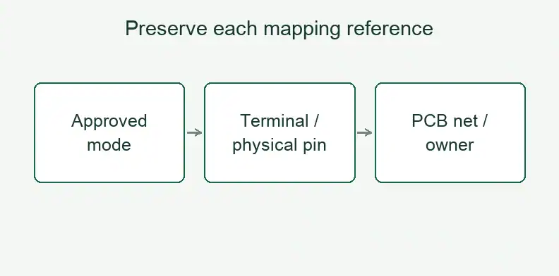
Quick Answer: HTRB and HTGB apply bias to different device terminals, so an order needs a separate approved terminal map for each mode. Tie the customer’s stress-plan revision to the device pin or pad, PCB net, slot orientation and board variant. Leave undefined connections on hold for the customer’s electrical or test owner.
A carrier can match its fabrication files while the loaded device or fitted variant differs from the intended test configuration. Before requesting a build, make that configuration readable alongside the PCB data.
Why do HTRB and HTGB need separate terminal maps?
The mode name does not fully describe the required connections. For a particular device, HTRB and HTGB can specify different gate-source and drain-source voltage states. The customer must translate those states into approved physical connections before the carrier goes to manufacture; the board supplier needs that released mapping to build against.
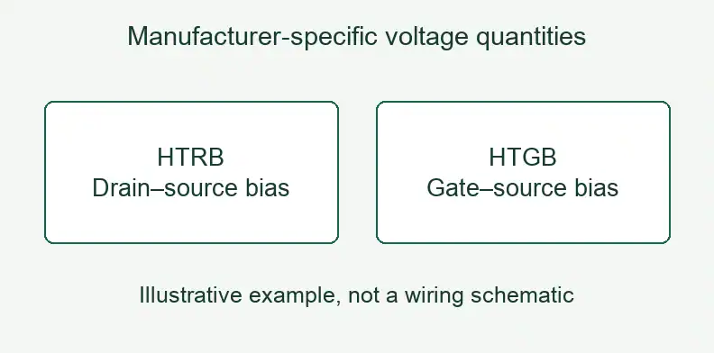
Mitsubishi Electric’s automotive SiC MOSFET reliability example makes the distinction visible. Its high-temperature reverse-bias (HTRB) example specifies VGS = 0 with drain-source bias. Its high-temperature gate-bias (HTGB) example specifies VDS = 0 with gate-source bias, including positive and negative gate conditions. These are the manufacturer’s example conditions for that device family.
The example explains why a single “bias board” label leaves questions open. It does not establish the voltage, polarity, temperature or duration for another part. Obtain those requirements from the applicable device documentation and customer-approved plan. Record each intended mode, including any polarity variant, against the exact part and package.
What does the carrier board actually do in these tests?
The carrier is a physical interconnect whose construction and fitted parts must support the customer’s released configuration. It can provide the device mounting and connections used within a larger stress setup. Ordering that PCB requires a defined board configuration, while the surrounding equipment and test plan retain their own requirements and owners.
EPC’s EPC2202–EPC2203 automotive qualification report, dated August 6, 2024, provides a concrete example. Its HTRB and HTGB sections identify devices mounted on FR5 adapter cards. The report describes an actual PCB adapter used with specified devices and conditions; it does not offer a generic carrier specification.
Use the report to establish the object being purchased, not to select material for a new design. FR5, the reported assembly details and the device-specific bias conditions belong to EPC’s example. A new purchase still needs its own stackup, fabrication drawing, device attachment and assembly definition. Confirm who supplies and fits the DUT if that work is separate from the carrier order.
What does “VGS = 0” mean on the board?
VGS = 0 describes the required voltage between gate and source. By itself, it does not specify how the circuit establishes that condition. The released design must show the intended connection and reference, with the customer resolving any ambiguity before fabrication or assembly. A net called GND does not answer that question.
A direct connection, an instrument-controlled state and another approved arrangement can imply different hardware. The Mitsubishi table does not identify which implementation a buyer should use. Do not infer a circuit from its voltage notation, or let a fabricator choose an implementation while preparing production data.
Ask the electrical owner to identify the gate, source and drain endpoints, the relevant return connection, and any fitted link or component involved. Apply the same discipline to VDS = 0. If a schematic note and assembly drawing disagree, hold the affected configuration for clarification. High-voltage insulation questions belong in the separate high-voltage PCB requirements review; a correct terminal map does not establish clearance, creepage or safety suitability.
What should go with the Gerber package for each mode?
Send a controlled connection record that makes the intended mode traceable from the customer plan to the board data. The fabricator should be able to identify which released drawing and netlist define the build. The customer’s electrical or test owner should approve the device-level meaning of those connections and resolve open items.
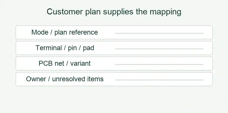
The following mode-to-terminal/net release record is an editorial suggestion for the RFQ package. It is not a test standard or a validated stress procedure. Use customer-approved values; a blank voltage field is a question to resolve, not permission to copy a manufacturer example.
| Record field | Information to supply |
|---|---|
| Device identity | MPN, package and applicable datasheet revision |
| Mode and authority | HTRB or HTGB, polarity variant and approved stress-plan revision |
| Required voltage states | Customer-defined VGS and VDS states, references and polarity |
| Physical connection | Each terminal → physical pin or pad → PCB net; supply and return endpoints |
| Zero-voltage implementation | Approved circuit reference and relevant fitted link or component |
| Release status | Drawing/netlist revisions, approving owner and unresolved items |
Keep the record connected to the controlled drawings. If a pad number changes, update the mapping reference rather than relying on an email explanation that never reaches the manufacturing package.
How can slots, keying and board variants change the intended connection?
A correct copper netlist can coexist with a wrong loaded configuration. Device orientation, slot identification or fitted links may differ from the arrangement the test owner approved. Reconcile the physical loading instructions and assembly variant with the mode record, so a check of bare-board connectivity is not mistaken for approval of the loaded setup.
Keep the assembly drawing specific about the viewing side and orientation reference. A slot label should lead to a particular terminal map, not merely a device family. Where fitted straps or jumpers distinguish modes, identify the approved population for each variant; do not ask an operator to infer it from a generic board name.
This suggested slot/variant reconciliation card is a second editorial tool, not a published standard. It records the identity of what will be loaded and the limits of the evidence available.
| Check item | Controlled reference or disposition |
|---|---|
| Slot and orientation | Slot ID, drawing view, key or silkscreen reference, terminal-map ID |
| Physical board | Board number and revision |
| Fitted variant | BOM revision and applicable strap/jumper population |
| Intended mode | Approved mode-record reference for this loading |
| Evidence and hold | Drawing/netlist check, agreed post-assembly check, customer setup validation or unresolved hold |
What can a board supplier verify, and what stays with the test owner?
A supplier can check the manufactured board against agreed fabrication and assembly requirements. The customer retains responsibility for selecting the stress conditions and approving how the carrier is used with the device and equipment. Put the requested checks and deliverables in the quotation so each party knows which evidence it will receive.
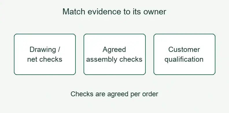
Under the QueenEMS ATE PCB manufacturing scope, the purchase starts from released customer design data, with assembly quoted separately when needed. Bare-board electrical testing can address connectivity against the agreed data. It cannot establish that the customer’s chosen pins, bias mode or loaded device orientation satisfy a qualification plan.
For an assembled order, agree which population, polarity and connectivity checks apply and how they will be recorded. Device qualification, stress execution and interpretation of device results remain with the customer’s test owner or appointed provider. A request for a carrier does not include those services. Unresolved device mapping should return to that owner before the affected build is released.
What else should buyers confirm before ordering? (FAQ)
Most remaining purchase questions concern configuration and scope: whether the same hardware supports both modes, which device requirements apply and who runs the stress test. Resolve these against the actual order. A generic carrier name or a manufacturer’s example report cannot settle them for a different device.
Can one carrier serve both HTRB and HTGB?
Possibly, if the customer’s released design and approved configuration support both. Record each mode and fitted variant separately. This article does not establish that a particular board can change modes safely or without rewiring.
Does a manufacturer’s example bias level apply to my device?
Do not transfer it by default. Use the requirements approved for the exact device and plan. Mitsubishi’s SiC example and EPC’s GaN report describe different devices and conditions, not a shared universal bias recipe.
Does the PCB supplier run the HTRB or HTGB test?
The manufacturing scope described here covers the carrier build and agreed checks. HTRB/HTGB stress testing and device qualification require a separate arrangement with the responsible test provider; they are not included in a QueenEMS PCB quotation.
Send your released files for a quote and free DFM review.
Send Gerber, drill files, stackup and drawings for a carrier PCB quote. Include approved mode, terminal, net and slot references.
For assembly, add the BOM and drawing. Agree board checks; HTRB/HTGB stress testing stays with the party running the stress test.