
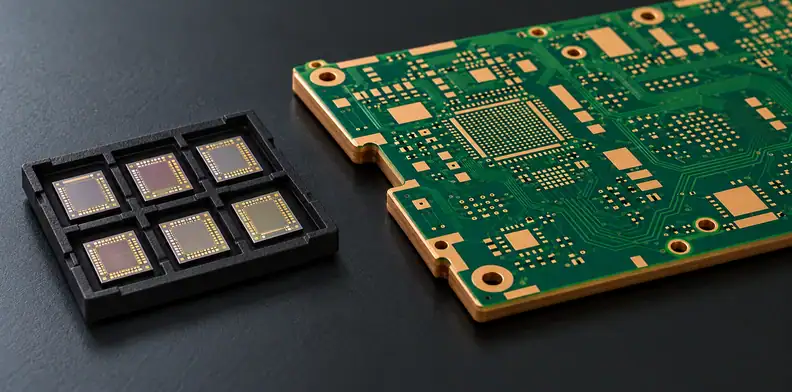
Quick Answer: For an embedded die PCB, known good die (KGD) release should name the die supplier, the provider of its semiconductor test evidence, and the embedding-process owner who accepts the delivered die format. The product owner approves the required grade, coverage and exceptions before release. Agree responsibility for additional preparation, loss, replacement and failure analysis in the order terms, because a KGD label alone cannot qualify the later embedding process.
An offer for unpackaged silicon can leave several different decisions inside the word “good.” You need to know what passed, when it passed, what happened afterward, and who accepts it for the proposed build. Settle those questions while the die and their evidence can still be examined separately.
Who supplies the die and who approves it?
Name three roles before release: the die source, the provider of the specified test evidence, and the owner accepting the incoming format into the embedding process. The product owner approves the requirements and evidence. Record whether the order uses customer-supplied die or supplier-arranged sourcing; an ordinary PCB quotation establishes neither arrangement.
One company may fill several roles, but the order should still identify each responsibility. The source supplying the die may rely on another party for testing or preparation. Ask which organization provides the report and which party can resolve a discrepancy before the die are committed to the build.
The JEDEC bare-die procurement page currently displays JESD49B.01, October 2023. Its public scope concerns bare and bumped die procurement, as-delivered expectations and application-data needs. That scope frames the discussion; it does not supply a verified contractual allocation for this order.
What separates tested die from known good die?
The offered grade and its reference specification determine what testing the supplier promises. A wafer-probe pass alone may describe less coverage than a known-good-die offer. Request the exact part, revision, grade and exceptions instead of accepting “bare die,” “tested” and “KGD” as interchangeable descriptions of the delivered semiconductor.
TI's die and wafer services overview provides a concrete manufacturer-specific distinction. Its tested die receive 25°C DC probing without special testing; its KGD are tested to the quality and reliability standards of corresponding packaged products. This is TI's taxonomy, rather than an industry-wide grade scale.
Etron's KGD explanation likewise describes tested unpackaged die against specified functionality, quality and reliability. Use the actual supplier's specification to define the offer. Record exclusions and conditional guarantees alongside the grade so the purchasing description and evidence mean the same thing.
Which test stage and coverage must the evidence identify?
The report should identify whether testing occurred at wafer level, after singulation or after integration, together with the applicable device specification, conditions and pass criteria. Different devices require different coverage. A test performed at one stage cannot describe changes introduced later unless the evidence or an agreed additional check addresses that later state.
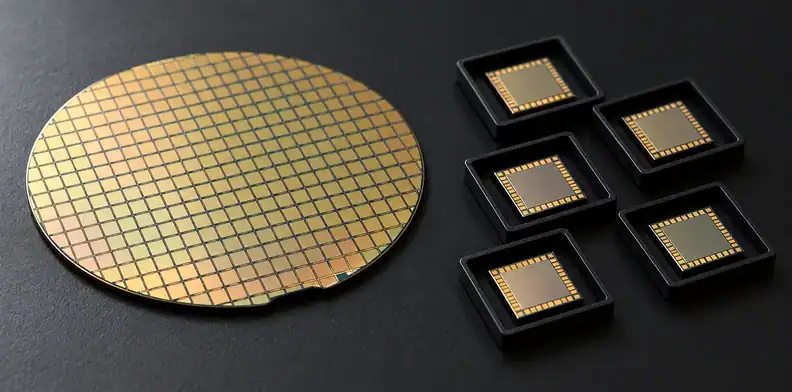
SPEA's KGD testing article distinguishes wafer screening, individual-die testing and package-level verification. Its SiC power-device example separates static, dynamic and short-circuit tests. That example shows why “electrically tested” needs detail; it is not a mandatory test list for logic or memory die.
Ask the evidence provider to connect each accepted bin to the relevant test program and specification revision. Identify conditions and exclusions that affect the intended application. Do not assume every KGD offer requires singulated-die testing, or that a final test performed after integration can substitute for evidence on the incoming die.
How do maps and preparation affect delivered-die evidence?
A wafer map can identify die locations and test bins, but the associated program and report explain what those bins mean. Track preparation after the recorded test, including any required sawing or handling. The release evidence should identify the state delivered and whether later operations require additional inspection or testing for the agreed order.
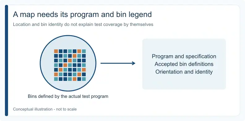
Semiprobe's probing explanation, dated February 2020, describes maps supporting multiple programs and bins. An ink reject means failure against that program's requirements; it need not mean a completely nonfunctional die. Preserve the bin legend and orientation rather than treating every map as self-explanatory.
The same source describes sawing that can introduce cracks, chip-outs or ESD damage to die that previously passed wafer probe, and notes that some customers retest singulated die. For your handoff, identify who performs any preparation and what evidence follows it. An earlier probe result and a newly received carrier should have a documented identity link where supported by the supplier's records.
Why does KGD status leave process fit unresolved?
Incoming semiconductor quality and compatibility with the embedding route require separate approvals. The proposed process must accept the delivered geometry, pad or bump format, surface condition and allowed exposure. Passing a die-vendor test does not answer whether the subsequent interconnection and embedding construction have been qualified for that device and application.
TI's historical SBOA147 technical note, ©2016, discusses varying bond-pad geometry and matching pad metallurgy and process parameters to the manufacturing approach. Use those physical inputs in the process-fit review; its historical product suffixes and yield examples are not current order guarantees.
The SMTA embedded-die RDL paper, Boettcher et al., 2021, reports a research demonstrator with interconnect work and a reliability issue needing optimization. It illustrates the separate process-qualification task. Keep inspection after lamination in the downstream inspection plan; formed embedded resistors and capacitors involve a different input-evidence question.
For a quotation that includes a free DFM review, provide Gerber data and the proposed stackup with the die specification, test-report summary and intended construction. Supply an assembly BOM when that work is requested. Feasibility and scope are reviewed for the specific project; die sourcing, screening and embedding responsibilities must be confirmed in writing before release.
Where should each release responsibility be recorded?
Record each responsibility beside the decision and evidence it must deliver, rather than assigning a vague “KGD approved” status to the whole supply chain. Name the party providing the input and the party accepting it. Resolve additional preparation, process fit and loss disposition explicitly so the release record does not hide gaps between suppliers.
This pre-embedding responsibility map is a suggested engineering/procurement aid. Responsibilities are negotiated per order; these rows are not a standard allocation or a statement that one fabricator performs every activity.
| Decision | Named party and evidence to agree |
|---|---|
| Semiconductor identity | Product owner approves part/revision/grade; source identifies delivered form and sourcing model |
| Meaning of KGD | Die supplier or test provider supplies specification, coverage, conditions, bins and exclusions; product owner accepts them |
| Preparation and retest | Actual preparation provider records required operations and evidence for the delivered state |
| Embedding compatibility | Process owner accepts geometry, interconnect format, handling and exposure; purchaser approves qualification scope |
| Loss and disposition | Contracting parties agree custody boundaries, quantities, hold/reject authority, replacement, scrap and failure-analysis route |
For a later failure, retain the evidence needed to distinguish incoming-die, handling and embedding-process questions. Payment and replacement responsibility follow the agreed terms and investigation route, rather than an assumed universal loss split.
When should the die handoff traveler release or hold?
Release only when the critical identity, test-state, preparation and process-fit inputs have an accepted disposition and a named sign-off. Hold when a critical input is missing or conflicts with the received die. A versioned traveler should connect the offered tested state to the received state and authorized quantity entering the embedding process.
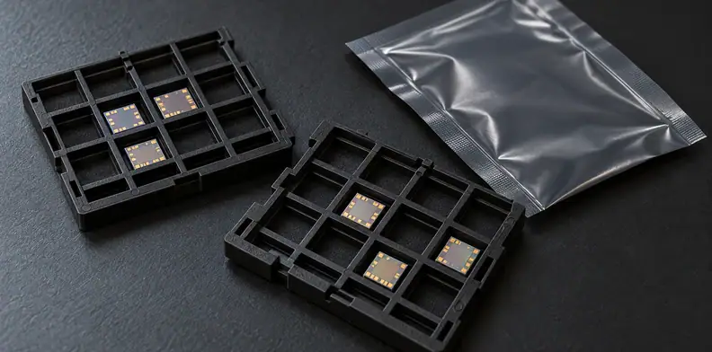
This die handoff traveler is a suggested engineering/procurement aid. Record the following against the order revision:
- Part/revision, supplier lot and supported wafer/die or equivalent identifiers.
- Available map, bin legend and orientation, linked test report and specification revision.
- Required preparation history, carrier and handling requirements.
- Received quantity, discrepancies and quantity authorized for release.
- Named approval or hold, disposition reference and responsibility for quantity reconciliation.
Provide fields for consumed, remaining and rejected quantities as the work proceeds, with their responsible owner. This is quantity reconciliation, not a substitute for downstream device-to-net test results. At the release gate, critical blanks remain open until accepted evidence or an authorized disposition closes them.
Frequently Asked Questions
Is a wafer-probed die the same as known good die?
Not automatically. The offered grade determines coverage. TI, for example, distinguishes room-temperature DC-probed tested die from its KGD offer tied to packaged-equivalent quality and reliability standards. Ask for the actual supplier's grade, specification and exclusions rather than treating the phrase “probe pass” as sufficient qualification.
Does KGD status mean a die will survive lamination?
No. Semiconductor test status and compatibility with a later embedding process answer separate questions. Match the delivered geometry, pad or bump format and allowed exposure to the intended route. The process owner must establish the applicable qualification evidence for that combination before the product owner releases it.
Can the PCB fabricator be responsible for die screening?
Yes, if that activity is explicitly contracted and the provider's capability and evidence are confirmed for the required screening. A routine PCB quote establishes no such responsibility. Name the actual test provider, coverage, report and acceptance authority; ordinary board inspection capability alone does not establish bare-die screening.
Who pays if an embedded die fails after lamination?
The agreed order terms determine the allocation, supported by the agreed failure-analysis route. Settle responsibility for replacement die, additional testing, scrap and investigation before release. Preserve the incoming test and preparation records so a later finding can be assessed against the supplied state and the relevant custody boundary. This is a planning point, not legal advice.
Does a JEDEC standard assign these responsibilities?
The public JESD49B.01 scope concerns procurement and use of bare or bumped die and as-delivered expectations. That scope alone does not verify a particular responsibility allocation. Read the applicable full standard and supplier specification, then state the actual parties and obligations in the order's agreed requirements.
QueenEMS has more than 10 years of experience. Request a quotation and free DFM review by sending the Gerber package, stackup and die documentation, including unresolved release inputs. Include an assembly BOM only when you request assembly, and confirm the construction and evidence scope before committing die.
Upload your files today · Free DFM check before production · Ship worldwide
Get your PCB prototypes in as fast as 24 hours. We handle FR4, Rogers, and hybrid boards, with standard builds up to 24 layers and higher layer counts subject to engineering review — free prototypes for 2–4 layer FR-4 boards, no minimum order.
Just upload your Gerber + BOM — we source every part, assemble, and inspect (AOI + X‑Ray) so you don't have to chase suppliers. PCB assembly typically takes 5–8 working days once all components are in stock. The confirmed delivery schedule is subject to your quotation.