Blog
PCB fabrication, PCB assembly, PCB materials, DFM, SMT, HDI, ceramic PCB, and electronics manufacturing guides from QueenEMS.
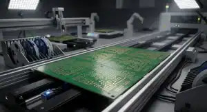
PCB Panelization for Assembly: Rails, Fiducials, V-Score and Tabs
PCB panelization for assembly means arranging several boards, or one small board, in an array with breakaway rails, fiducials and tooling holes…
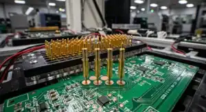
How to Prevent a $4,500 PCB Redesign Due to Poor Test Access
Table of Contents Getting a printed circuit board manufactured is only the beginning; verifying that it functions correctly dictates your project’s success….

How to Choose a Cost-Effective PCB Assembly Test Strategy
Table of Contents Choosing a test strategy for PCB assembly is not just a quality decision—it is a financial one. If you…
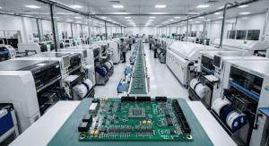
How to Scale PCB Assembly From Pilot to Mass Production Without Yield Collapse
Quick Answer: Scale PCB assembly by treating the pilot as a production-system test, not only a functional board test. Release volume after…
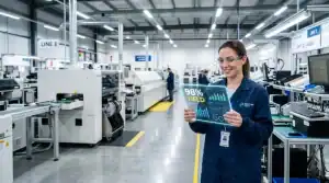
How to Judge CMs by PCB Assembly First Pass Yield
Table of Contents An accurate pcb assembly first pass yield tells you exactly how many boards rolled off the line perfectly the…

How to Route Fine-Pitch BGA Fanout HDI PCB Like a Pro
Table of Contents Hardware engineers face severe routing bottlenecks when component densities shrink. You might successfully place a 0.4mm processor on your…
How to Apply Ceramic PCB Design Rules: 12 DFM Checks
Twelve ceramic PCB design rules for trace/space, pads, vias, copper balance and edge clearance, built to reduce DFM questions before fabrication….

How to Use an HDI PCB DFM Checklist for Layout
Table of Contents You finish routing a dense 0.4mm BGA, send the manufacturing files to fabrication, and immediately get hit with an…
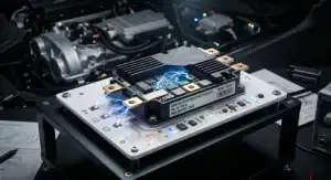
Ceramic PCB for 800V EV Power Electronics: How to Choose
Choose ceramic PCB materials for 800V EV power electronics by isolation, thermal cycling, SiC compatibility and substrate fit for traction modules….
Ceramic PCB vs Metal Core PCB: Compare Thermal Paths
Compare ceramic PCB vs metal core PCB by complete thermal paths, insulation, geometry and cost. Calculate a thermal budget without a universal 5W cutoff….

HDI Stackup Types: How to Choose 1+N+1, 2+N+2, or ELIC PCB
Table of Contents HDI stackup types determine your board’s physical architecture, routing density, and manufacturing cost based on microvia placement. You start…

How to Decide When to Use HDI PCB in Layout: 7 Signals Your Standard Multilayer Design Has Reached Its Limit
Table of Contents Starting a dense board layout only to realize halfway through that you have run out of routing space is…