
Blog
PCB fabrication, PCB assembly, PCB materials, DFM, SMT, HDI, ceramic PCB, and electronics manufacturing guides from QueenEMS.
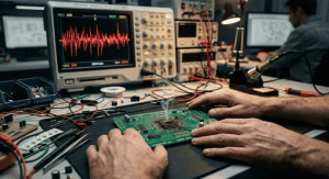
7 Reasons for PCB Prototype Failure (And How to Prevent Each One)
You open the shipping box, plug in your freshly assembled board, and… nothing happens. Or worse, you see the magic smoke. A…

PCB DFM: The Complete Design for Manufacturing Checklist (With Real Factory Examples)
You just finished routing a dense 4-layer board, passed the design checks with zero errors, and sent it to the factory. Three…

How China vs USA PCB Assembly Choices Work
China vs USA PCB assembly compared by build stage, landed cost, sourcing control, quality evidence, testing scope, and release-package maturity….
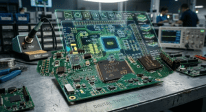
What PCB Assembly Quote Files Do You Actually Need?
Table of Contents You just finished routing your board and sent the design off to three different manufacturers. One replies with a…
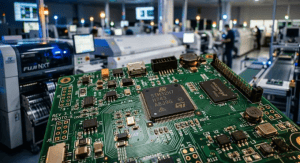
PCB Assembly Cost Breakdown: How to Budget for Your Next Project
You have sent your Gerber files to three different suppliers and received three wildly different quotes. One says $800, another says $2,400,…

How to Create a Flawless BOM for PCB Assembly (Free Template)
You just finished your board design, generated the files, and hit send. But if your BOM for PCB assembly is messy, you…
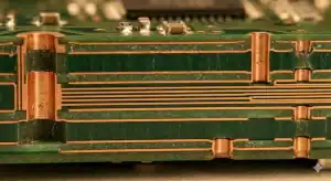
Prepreg PCB Guide: 10 Secrets To Flawless Board Stackups
The material known as prepreg is a dielectric insulator made of woven fiberglass impregnated with partially cured epoxy resin. Are unpredictable impedance…
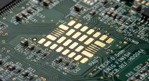
How to Prevent Black Pad on Your ENIG Surface Finish Boards
You receive a batch of assembled printed circuit boards, only to find the ball grid arrays failing during thermal cycling tests. This…
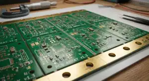
How PCB Panel Costs Change Your Quote
Quick answer: PCB panel costs go down when the panel fits more usable boards without creating assembly, inspection, or depaneling risk. The…

Stop PCB Failures: The Flying Probe Test Survival Guide
You design complex high-density circuit boards daily. Hidden manufacturing defects routinely ruin product launches without proper verification. These invisible errors cause catastrophic…
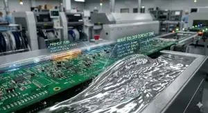
Why Your Wave Soldering Fails: The Ultimate Process & DFM Guide
Making sense of wave soldering means understanding how a cascading pan of molten solder perfectly secures thousands of through-hole components to a…
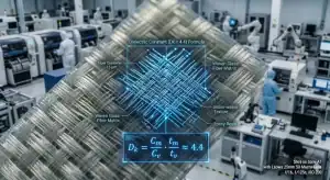
How to Choose FR4 Material: Tg 130, 150 or 170?
You can save up to 30% on bare board manufacturing costs by matching your printed circuit board’s thermal profile to the exact…