

Quick Answer: PCB annular ring breakout is not judged from one top-side photograph. Acceptance depends on the product class and standard revision, external versus internal layer, remaining conductor at the land junction, electrical spacing, plating integrity, feature type, and evidence that shows the direction and extent of misregistration.
Key takeaways – Design annular ring and finished-board breakout are related but different decisions. – External visual inspection cannot reveal the minimum ring on buried layers. – Class 1, Class 2, and Class 3 requirements must be named in the purchase package. – Microsection, registration coupons, correlated CAM data, or other approved methods may be needed to disposition a lot.
PCB annular ring breakout becomes a supplier dispute when a drilled hole appears off-centre, yet nobody has agreed which layer, product class, measurement basis, or conductor condition controls acceptance. The buyer sees a crescent of copper on the surface; the fabricator sees registration within a process distribution; the design engineer worries that a trace or plane connection may be cut internally.
QueenEMS already has an annular-ring design article with sizing formulas and a second page on optimising annular ring for manufacturing. This article owns the later decision: how to evaluate breakout on fabricated boards, what evidence can release a lot, and how to prevent the same ambiguity in the next RFQ.
Table of Contents
- Define the acceptance basis first
- Separate external and internal evidence
- Find the cause of the offset pattern
- Check the land-to-conductor junction
- Choose evidence for the hidden layers
- Decide whether the lot can be used
- Recover margin in the next revision
- Make breakout review quote-ready
Define the acceptance basis first
Breakout can be accepted only against a named printed-board requirement. The purchase drawing should identify the applicable IPC-6012 revision for rigid boards, product class, customer additions, via or plated-through-hole type, and any stricter annular-ring note.
Do not mix design guidance with finished-board acceptance. IPC-2221 helps designers size lands with fabrication allowance, while IPC-6012 addresses qualification and performance of finished rigid boards. A CAD rule can provide generous nominal copper and still produce a nonconforming lot if registration shifts beyond the agreed limit. Conversely, a hole that looks visually off-centre may remain acceptable under the ordered class and feature condition.
The standard revision matters because details and measurement definitions evolve. Public summaries often reduce the rules to “Class 2 allows breakout and Class 3 does not,” but the actual decision also considers layer location, conductor-width reduction, microvia contact, spacing, plating, and stated exceptions. Use the controlled standard and contract documents rather than a graphic copied from a blog.
Record the feature population under review: component holes, vias, press-fit holes, blind or buried vias, microvias, and nonfunctional pads do not all carry the same connection geometry. Finished-hole and drilled-hole references also differ by external or internal measurement.
Contract rule: No breakout concession should be approved until the standard, revision, class, feature, and affected layer are identified.
Separate external and internal evidence
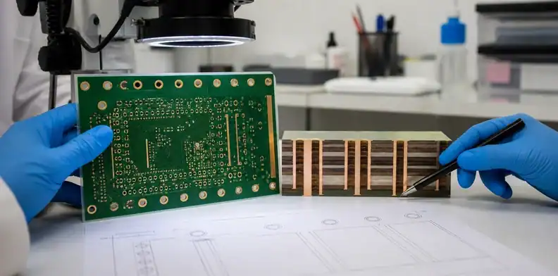
External annular ring can often be evaluated by optical inspection because the finished pad and plated hole are visible. Internal annular ring is hidden inside the stack-up and may need cross-sectioning, coupons, radiography, electrical structures, or a correlated registration method.
On an external layer, measurement is commonly referenced from the finished plated-hole wall to the edge of the land. On an internal layer, the drilled hole boundary and internal land relationship govern the remaining copper. Plating thickness changes the visible opening, so a surface photograph should not be used to calculate an unseen internal ring.
Look at offset direction across multiple holes and locations. A random single-hole event suggests a different cause from a consistent panel shift, radial movement, layer-specific scale error, or drill pattern offset. The direction can indicate which internal land-to-trace junction or clearance region is at risk.
Outer-layer acceptance also needs the whole land. A narrow crescent may still retain a strong conductor junction, while another orientation can cut directly into a trace neck. Inspect solder mask registration, pad lifting, nicks, plating folds, and hole-wall damage so an annular-ring review does not ignore adjacent defects.
| Observation | What it can prove | What remains unknown |
|---|---|---|
| Top-side macro image | External hole-to-land position | Buried-layer registration |
| Bottom-side image | Opposite external relationship | Internal scale and skew |
| Hole-size measurement | Finished opening and tolerance | Minimum internal copper |
| Electrical continuity | Connection exists at test time | Remaining junction width and life margin |
| Stack-up registration evidence | Layer alignment distribution | Local plating condition unless separately inspected |
The evidence plan should close the unknown column instead of adding more photographs of the same surface.
Find the cause of the offset pattern
Annular-ring loss usually comes from the tolerance stack between land size, artwork position, layer movement, drilling, and plating. Identifying the dominant pattern determines whether the correction belongs in CAD, CAM scaling, lamination, drill registration, tooling, or inspection.
Drill wander can move individual holes. Layer-to-layer misregistration can shift one internal image relative to the drill. Lamination changes dimensions and may create scale or skew by material direction. Artwork compensation that does not match the construction can produce repeatable panel patterns. Tool wear, entry material, stack height, spindle condition, and panel movement can add local drilling variation.
The design contributes when nominal ring leaves little room for those effects. A pad diameter calculated only from finished hole plus desired ring omits manufacturing allowance. Dense escape routing may also place a trace junction or adjacent copper exactly where the worst shift occurs.
Use panel maps rather than isolated defect counts. Mark row, column, side, layer where known, hole size, tool number, and offset direction. Compare production panels, registration coupons, and drill groups. A coherent map lets the supplier distinguish random drill behaviour from systematic scaling or tooling error.
High-layer builds add cumulative registration challenges. The hybrid PCB layer-registration review should identify sensitive land arrays and evidence before the first lot, especially where small annular rings coexist with sequential lamination or unusual materials.
Cause boundary: Corrective action should match the observed distribution; enlarging every pad does not fix a process-scale error, and drill tuning does not fix undersized CAD lands.
Check the land-to-conductor junction
The remaining conductor at the land junction is often more important than the breakout angle alone. Misregistration can reduce the trace or plane connection, threaten electrical spacing on the opposite side, or remove copper that supports the plated barrel knee.
Review the breakout direction against each connected feature. A hole shifted away from the attached trace may preserve its neck while losing nonfunctional copper. The same magnitude toward the trace can reduce the junction sharply. For plane connections, verify thermal-relief spokes or solid connections on the affected internal layer.
Teardrops can add copper at trace-to-land transitions, but they do not change the ordered class or erase a finished-board defect. Supplier-added teardrops are a CAM modification and need an agreed scope. The PCB teardrop approval article covers exclusions for impedance, RF, spacing, and released-artwork control.
Spacing must be checked simultaneously. A shifted hole and its plated barrel can approach adjacent copper even when the target land still has enough connection. High-voltage nets, dense plane antipads, or fine-pitch escape regions may be controlled by clearance before annular ring becomes the limiting criterion.
Plating integrity remains separate. Continuity through a reduced junction does not prove adequate hole-wall copper, corner condition, or thermal reliability. Include plating and microsection requirements already owned by the order.
Connection call: A permissible angle cannot release a feature that violates minimum conductor width, clearance, or plated-hole integrity.

Choose evidence for the hidden layers
Internal breakout should be evaluated with a method capable of showing or reliably predicting internal registration. The chosen method must be qualified for the board construction and correlated to physical results.
Microsectioning can directly reveal selected hole-to-land relationships and plating condition. Section orientation matters: a cut through the wrong axis can miss the minimum remaining ring. The report should identify panel, coupon, feature, layer, cut direction, magnification, measurement reference, and result. Use the PCB microsection report requirements to control traceability, then add the breakout-specific rotation and junction view.
IPC-6012F also recognises that internal registration may be assessed with approved techniques such as special patterns, probes, software correlated to pattern skew, radiographic methods, or electrically testable coupons. Correlation and calibration are the key words. A CAM prediction that has never been compared with physical sections is not automatically acceptance evidence.
Sampling should reflect distribution. If panel mapping shows a directional extreme, select sections at the risk location rather than only at the centre coupon. For a layer-specific scale concern, inspect the layer and panel positions that the analysis identifies. Preserve enough boards to verify any proposed sort.
| Evidence method | Strength | Limitation to control |
|---|---|---|
| Rotated microsection | Direct local geometry and plating view | Destructive and sample-limited |
| Registration coupon | Tracks panel and layer movement | Must represent product features |
| Radiographic analysis | Non-destructive alignment information | Resolution and interpretation need validation |
| Correlated CAM/software | Broad statistical coverage | Requires physical correlation and calibration |
| Electrical test structure | Detects designed connection or spacing failures | Does not directly show remaining copper shape |
Evidence rule: Use a method that can see the minimum-risk orientation and show its correlation to the shipped product.
Decide whether the lot can be used
Lot disposition should combine conformity, function, reliability consequence, distribution, and the strength of the available evidence. The outcomes are not limited to “accept everything” or “scrap everything.”
Start by containing panels or date codes associated with the pattern. Confirm product class, affected layer and hole family, measured extent, conductor and clearance condition, plating result, electrical test coverage, and whether the feature is connected or nonfunctional. Then identify which requirement is unmet and whether customer approval is mandatory.
A use-as-is deviation can be considered only when engineering can show that the named quantity remains functional and acceptable for the product. It should record the board revision, lot, panel range, feature, standard clause or drawing note, evidence, risk assessment, approval signatures, and repeat-order treatment. It must not silently lower the future baseline.
Sorting may be practical when a validated non-destructive method separates conforming and suspect boards. Destructive sections alone cannot sort every unit. Rework is usually limited because internal registration cannot be moved after lamination and drilling; proposals to redrill or enlarge holes must account for plating, finished size, annular ring, and component fit.
Customer-controlled Class 3 or high-reliability products often leave little room for informal concessions. Notify the customer or design authority according to the contract before consuming boards. Purchasing should also record replacement schedule, containment cost, and whether assembly materials have already been allocated.
Lot decision: Approve only the population supported by the measurement method and signatures; evidence from one panel cannot clear an unbounded shipment.

Recover margin in the next revision
Prevention starts by allocating enough land diameter for finished hole, required remaining ring, fabrication allowance, and the selected supplier’s process capability. The design should also protect the trace junction and adjacent clearances under worst-direction movement.
Review pad stacks by hole family rather than applying one global via rule. Component leads need finished-hole fit and solder flow. Signal vias trade land size against routing density. Press-fit holes add connector requirements. Blind vias, buried vias, and microvias use different drilling and capture-pad processes.
Where routing allows, increase lands, move adjacent copper, adjust antipads, add approved teardrops, reduce drill diameter without violating aspect ratio or finished-hole needs, or change via technology. Dense BGAs may need layer-count, via-in-pad, sequential-lamination, or escape-strategy changes rather than an impossible mechanical-drill tolerance.
Ask the fabricator for design and finished-board capability separately. A minimum nominal annular ring rule in CAD is not the same as guaranteed remaining ring after registration. Capture the agreed fabrication allowance in the DFM record, and recheck it after stack-up, material, layer count, drill source, or production-site changes.
First-article evidence should target the new margin. Use panel registration data, sections, or approved coupons to show that the correction works across the process distribution. Do not close corrective action because the next sample photograph happens to look centred.
Revision rule: Recover margin at the land, junction, and clearance together; moving risk from breakout to an adjacent short is not a fix.
Make breakout review quote-ready
The RFQ package should include Gerber or ODB++, NC drill files, fabrication drawing, drill table with finished and non-plated status, stack-up, pad stacks, product class, applicable IPC revision, critical hole families, annular-ring requirements, teardrop permissions, and the requested registration evidence.
Highlight locations where routing density leaves little margin and state whether the supplier may adjust pads or add copper during CAM. Name excluded nets and features. Require a marked-up proposal before any change to released data. Two suppliers can then quote the same geometry rather than applying different silent DFM edits.
Define first-lot and shipment evidence separately. First-lot qualification may include layer-registration coupons, rotated microsections, panel maps, or correlated software output. Repeat orders may need only normal process records unless material, stack-up, tooling, site, or drill geometry changes.
A fabrication note can state:
Build the plated-hole structures to the specified product class and drawing requirements. Review minimum annular ring, land-junction width, and drill-to-copper clearance using the released drill and pad data. Submit any proposed pad, teardrop, or drill change for approval and provide the agreed first-lot registration evidence.
For a QueenEMS quote, send the finished-hole table, pad-stack export, critical-layer images, stack-up, class and standard revision, panel quantity, allowed CAM edits, and requested section or registration report via the QueenEMS engineering contact page. The response can identify marginal features, proposed fabrication allowance, evidence scope, and any design decision that must close before tooling.
Quote boundary: A production-ready price includes the ordered class, actual hole families, allowed CAM changes, and a defined way to verify internal registration. Review our PCB quality control capabilities.

FAQ
Can a Class 2 PCB have annular ring breakout?
Yes, controlled breakout may be permitted in defined conditions under the applicable IPC-6012 requirements, but the remaining conductor, clearance, feature type, and layer still matter. Use the exact ordered revision instead of a simplified internet chart.
Can a surface photograph prove internal annular ring?
No. It shows an external hole-to-land relationship. Internal registration needs a suitable section, coupon, radiographic method, electrical structure, or validated correlated analysis.
Does passing electrical test make breakout acceptable?
No. Continuity and isolation at test time do not establish remaining junction width, product-class conformity, plating condition, or thermal reliability. Electrical test is one part of the evidence package.
Can the fabricator add teardrops without approval?
Only when the purchase package already authorises that DFM change and defines excluded regions. Otherwise, adding teardrops changes released copper artwork and should be approved through CAM review.
Sources
Written by the QueenEMS Engineering Team
Upload your files today · Free DFM check before production · Ship worldwide
Get your PCB prototypes in as fast as 24 hours. We handle FR4, Rogers, and hybrid boards up to 40 layers in volume production, with advanced builds subject to engineering review — free prototypes for 2–4 layer FR-4 boards, no minimum order.
Just upload your Gerber + BOM — we source every part, assemble, and inspect (AOI + X‑Ray) so you don't have to chase suppliers. Boards ship in as fast as 24 hours.