

Quick Answer: PCB cosmetic acceptance criteria should tell the receiving team which visible marks are acceptable, which marks need review, and which marks should stop the lot. The rule should name the inspection basis, product class, affected area, photos needed, affected quantity, and final disposition before the buyer accepts, rejects, sorts, or asks the supplier for a corrective action.
Key takeaways
- Use PCB cosmetic acceptance criteria to separate appearance-only variation from solderability, copper, insulation, marking, and customer-facing risks.
- Do not reject a PCB lot only because it looks different; first check location, size, affected count, and whether the mark reaches a functional area.
- Put the accepted cosmetic rule into the next RFQ so the same dispute does not repeat on a reorder.
A cosmetic dispute usually begins after the boards arrive. Someone opens the carton, sees scratches, stains, solder mask color variation, edge marks, exposed-looking copper, or unclear silkscreen, and asks a simple question: “Can we use these boards?”
That question is not really about beauty. It is about whether the visible condition changes soldering, electrical reliability, assembly fit, inspection, customer acceptance, or the agreed drawing. A small mark on a breakaway rail may not matter. The same mark on a gold finger, test pad, fine-pitch land, press-fit hole, or customer-facing surface may stop the lot.
Good cosmetic acceptance rules help the buyer make that decision without emotional arguments. They give engineering, quality, purchasing, receiving, and the supplier the same language for accept, sort, rework, concession, replacement, or future RFQ control.
Table of Contents
- Start with where the mark is located
- Name the inspection basis before the lot arrives
- Protect soldering and contact surfaces first
- Use photos and affected counts before rejecting
- Turn repeated cosmetic issues into RFQ wording
- Separate cosmetic concession from corrective action
- Keep the accepted cosmetic rule for the next order
Start with where the mark is located
The first cosmetic question is location. A mark on a nonfunctional rail, panel border, tooling area, or inner packaging surface is very different from a mark on a solder pad, plated hole, controlled contact, edge connector, fiducial, barcode area, or visible customer-facing surface.
Receiving teams sometimes lose time because the first discussion is too broad: “The boards are scratched.” A better discussion is: “Three boards have short solder mask scratches on the panel rail; no copper is exposed in the circuit area.” That wording gives quality and engineering something they can judge.
Use PCB incoming inspection as the place where this decision starts. Incoming inspection should not only count boards. It should identify whether the observed condition touches a functional feature, drawing note, customer appearance requirement, or assembly operation.
The buyer can use a simple location map:
| Location of cosmetic mark | Typical buyer action |
|---|---|
| Panel rail or breakaway area | Usually review only when it affects depaneling, label, or handling |
| Solder pad, BGA land, via-in-pad, or test pad | Hold for engineering or supplier disposition |
| Edge connector, gold finger, press-fit hole, or contact area | Treat as functional risk until proven acceptable |
| Silkscreen or polarity marking | Review when readability affects assembly or service |
| Customer-facing exposed board surface | Compare against the product appearance requirement |
This approach keeps the conversation practical. The buyer is not asking whether a board looks perfect. The buyer is asking whether the visible condition changes how the board will be assembled, tested, used, sold, or accepted.
For example, a small solder mask shade difference between lots may be acceptable for an internal controller board. The same variation may be a problem for a visible user-interface board if the customer has already approved a sample. The correct answer depends on product use, not only on the color.
The RFQ should make that use visible. If the board is a demo sample, a medical enclosure interface, a customer-visible control panel, or a replacement part that must match a previous lot, say so before fabrication. Otherwise, the supplier may quote a normal industrial appearance standard while the buyer expects a stricter cosmetic result.
Name the inspection basis before the lot arrives
PCB cosmetic acceptance criteria should point to an inspection basis before the boards ship. The basis may be IPC-A-600 for bare printed boards, IPC-A-610 for assembled electronic assemblies, a customer drawing note, a golden sample, or a project-specific receiving rule.
The mistake is to argue from memory after the lot arrives. One person may say a mark is normal process variation. Another may call it a defect. Without a named basis, both sides can sound reasonable while the lot sits unused.
For bare boards, many buyers refer to IPC-A-600 acceptance concepts. For assembled boards, the inspection conversation often changes because components, solder joints, cleanliness, and assembly damage enter the decision. The article should not treat all cosmetic marks as one category.
When shipment evidence is needed, connect the requirement to PCB quality documents before shipment. That page helps define which inspection report, photo set, certificate, packing proof, or lot record should travel with the shipment.
Use RFQ wording like this:
“Cosmetic acceptance basis: bare PCB to IPC-A-600 Class 2 unless drawing notes are stricter. Hold for approval if visible marks affect solder pads, edge connectors, fiducials, readable markings, customer-facing surfaces, or any condition shown in the approved sample.”
That sentence does several useful things. It names the baseline. It protects the areas that matter. It gives the supplier a hold trigger. It also prevents the buyer from rejecting every harmless process mark after the boards arrive.
If the product has special appearance needs, include a photo reference or sample boundary. A written note such as “green solder mask only” is not the same as a defined color tolerance, surface appearance standard, or approved sample. If the exact look matters, the supplier needs to know that before quotation.
The goal is not to create a difficult inspection document for every simple board. The goal is to define the few appearance issues that would change acceptance. A normal industrial control board may need only a short note. A visible consumer-facing PCB may need photo examples and a stricter acceptance boundary.
Protect soldering and contact surfaces first
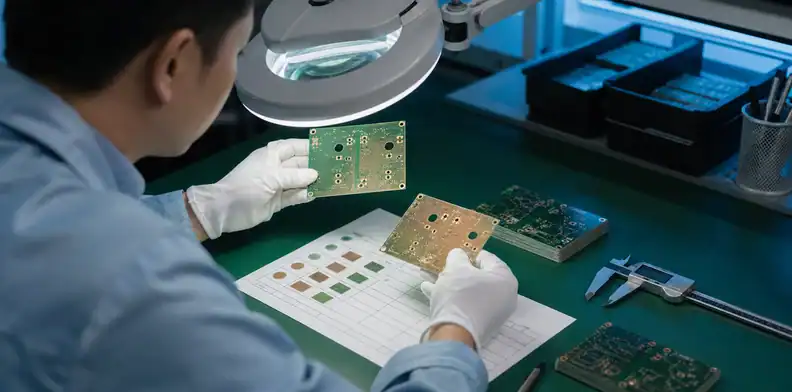
The highest-risk cosmetic issues are the ones that touch soldering, electrical contact, insulation, or assembly alignment. A board can look acceptable at a distance and still create trouble if a mark affects pads, exposed copper, plating, or mask clearance near fine-pitch parts.
Receiving should pay close attention to solder pads, BGA lands, edge connectors, gold fingers, plated holes, press-fit areas, fiducials, test pads, and any area used by automated optical inspection. Cosmetic variation in those places can become an assembly or reliability question.
Use PCB solderability test for bare boards when the visible condition raises doubt about wetting, oxidation, storage damage, or finish quality. Solderability is not proven by appearance alone, but appearance can tell the team where to investigate.
Practical receiving logic looks like this:
| Observed condition | Better first question |
|---|---|
| Light scratch on solder mask | Does it expose copper or reach a controlled area? |
| Discoloration on finish | Does it affect solderability or contact performance? |
| Mask nick near fine-pitch pads | Does it change solder bridge or insulation risk? |
| Silkscreen smear | Does it hide polarity, reference designator, or service marking? |
| Edge damage | Does it affect board outline, connector fit, or customer appearance? |
The supplier should not be asked to defend every small mark. The buyer should first identify whether the mark changes use. That makes the claim fairer and faster.
For PCBA work, this distinction matters even more. A bare board scratch that would be harmless on a panel rail may become a serious issue if it prevents correct placement, hides a polarity mark, or interferes with a test probe. If assembly will happen at QueenEMS or another EMS supplier, the receiving rule should protect the assembly operation, not only the bare board appearance.
Quality should also avoid accepting a cosmetic concession that conflicts with the end customer. If the final customer sees the board, handles the board, photographs the board, or uses the board as a service replacement, cosmetic expectations belong in the RFQ package, not in a complaint after delivery.
Use photos and affected counts before rejecting
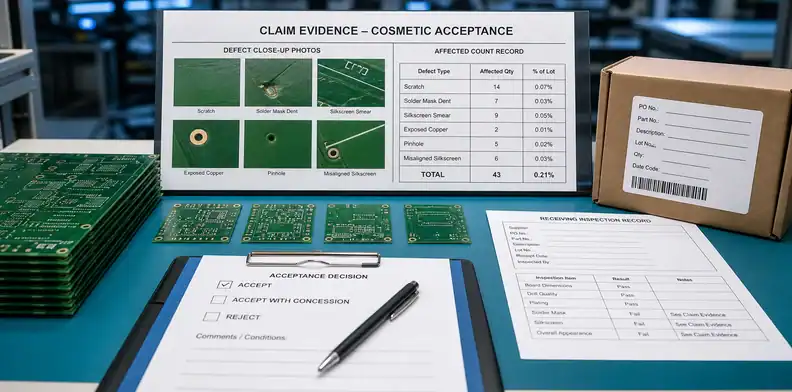
A cosmetic claim needs photos, location, affected count, lot information, and requested disposition. Without those details, the supplier may not be able to decide whether the issue is a process indicator, shipping damage, handling damage, isolated defect, or lot-wide condition.
Good photos show the full board, the local feature, the scale of the mark, the board side, and the lot or packing context. A single close-up photo can make a harmless mark look worse than it is. A distant photo can hide a real defect. Use both.
If packing may have contributed to the issue, link the claim to PCB packaging requirements. Scratches, corner dents, label confusion, moisture exposure, or tray movement can come from handling after fabrication, not only from the PCB process itself.
The claim should include:
- PO or quote number
- Board part number and revision
- Lot quantity and affected quantity
- Board side and location
- Clear photos with scale or reference
- Whether the boards are unused, assembled, tested, or already handled
- Requested action: accept with note, sort, replace, rework, credit, or root-cause review
This does not need to become paperwork theatre. It simply gives the supplier enough information to respond without guessing.
For example, “12 of 200 boards show solder mask scratches near J3 on the top side; copper is not visible; please confirm acceptability before assembly” is much more useful than “boards scratched, please advise.” The first version allows a disposition. The second version creates another email round.
When the buyer wants a replacement or corrective action, connect the issue to PCB supplier quality claim evidence. A claim is stronger when it includes both the observed condition and the business decision: whether production is held, whether sorting is allowed, whether urgent replacement is needed, and whether future lots need a tighter note.
Turn repeated cosmetic issues into RFQ wording
Repeated cosmetic disputes should become clearer RFQ language. If the same appearance issue appears on more than one order, the buyer should stop relying on complaint emails and add the acceptance boundary to the next quote package.
The next RFQ should tell the supplier what matters, not just what was disliked last time. Useful wording includes the affected area, the allowed condition, the inspection basis, and the hold trigger.
Examples:
- “No exposed copper or mask scratch allowed on solder pads, edge connector contacts, fiducials, or customer-facing top surface.”
- “Solder mask shade variation is acceptable if solderability, marking readability, and customer-facing appearance are not affected.”
- “Silkscreen must remain readable for polarity, connector labels, and service markings.”
- “Photo confirmation required before shipment for first repeat lot after cosmetic claim.”
These notes are short, but they change the supplier’s quoting assumptions. If the requirement is stricter than normal, the supplier can plan inspection, handling, packing, or cost before production starts. If it is not stricter, the buyer has a record that prevents unnecessary rejection.
For a PCB-only project, send QueenEMS the Gerber or ODB++ data, drawing, surface finish, product use, previous lot photos, affected-count record, and the cosmetic condition that caused concern. For a PCBA project, also include assembly drawing, component placement risk, test or contact areas, and whether the board will be visible to the final customer.
QueenEMS can review whether the cosmetic issue belongs in incoming inspection, supplier claim handling, future RFQ wording, or assembly risk review. That review helps the buyer avoid two bad outcomes: rejecting usable boards or accepting boards that create soldering, test, or customer problems later.
Before sending the next RFQ, turn the dispute into one short buyer instruction. A practical note might say: “For this visible top-side product, hold for approval if scratches, mask damage, stains, or silkscreen defects affect customer-facing areas, solder pads, fiducials, polarity marks, edge connectors, or packing-label traceability. Provide photos before shipment for any condition outside normal process appearance.” This kind of wording is much easier for a supplier to price and inspect than a general request for “good appearance.”
For purchasing, the useful test is simple: can a new receiving inspector apply the rule without reopening the whole email history? If the answer is yes, the cosmetic criteria are ready for quote and repeat-order control.
Separate cosmetic concession from corrective action
A cosmetic concession says whether one visible condition can ship. Corrective action asks why the condition happened and how the supplier will reduce recurrence. Keeping those two decisions separate helps the buyer avoid turning every small mark into a formal quality dispute while still protecting repeat orders.
A practical RFQ note can say that isolated non-functional marks may be reviewed by photo, but repeated marks in the same location, near contacts, or near soldering areas require supplier feedback before the next lot.
- Concession: can this lot be accepted as-is?
- Containment: are more boards affected than shown?
- Correction: what process step created the mark?
- Next order: what evidence or inspection rule changes?
Keep the accepted cosmetic rule for the next order
Once a buyer accepts or rejects a cosmetic condition, the decision should stay with the quote file. Repeat orders become difficult when the first lot was accepted by informal email and the next inspector applies a different rule.
The useful record is short: photo, affected location, quantity, accepted limit, decision owner, and whether the rule applies only to that lot or to future production. That creates experience-based evidence without pretending that every cosmetic issue has the same risk.
- Reference photo or sample board
- Functional area affected or not affected
- Accepted quantity or defect limit
- Lot-only decision or repeat-order rule
FAQ
Are PCB color variations always defects?
No. Color variation is often acceptable when it does not affect solderability, marking readability, customer-facing appearance, or an agreed sample. It should be reviewed when the product has a defined appearance requirement.
Should I reject a PCB lot for scratches?
Reject only after checking location, size, affected quantity, copper exposure, functional risk, and the agreed inspection basis. A scratch on a rail is not the same as a scratch on a solder pad or contact area.
Does IPC-A-600 cover assembled boards?
IPC-A-600 is used for bare printed board acceptability. Once components and solder joints are involved, assembly acceptance usually needs IPC-A-610 concepts or project-specific assembly criteria.
What photos should I send for a cosmetic claim?
Send one full-board photo, close-ups with scale, board side, location, affected quantity, lot label, packing condition, and the requested disposition. The supplier needs enough context to decide whether the lot can be accepted, sorted, replaced, or corrected.
Can QueenEMS help decide if a cosmetic issue affects assembly?
Yes. Send the board photos, Gerber or ODB++ data, drawing, lot quantity, affected count, and assembly or customer-use context. QueenEMS can help identify whether the issue is appearance-only, assembly-related, or a future RFQ control point.
Sources
- IPC-A-600M official standard page – used for current bare-board acceptability context.
- IPC standards overview – used as standards-background context.
Send QueenEMS a quote-ready cosmetic review package
If your PCB or PCBA project has a visible-board concern tied to PCB cosmetic acceptance criteria, send QueenEMS the board photos, Gerber or ODB++ files, fabrication drawing, surface finish, lot quantity, affected quantity, packing label, product-use context, and any customer appearance requirement. We can help review whether the lot should be accepted, sorted, disputed, or controlled in the next RFQ.
Written by the QueenEMS Engineering Team
Upload your files today · Free DFM check before production · Ship worldwide
Get your PCB prototypes in as fast as 24 hours. We handle FR4, Rogers, and Flex up to 60 layers — free prototypes for 2–4 layer boards, no minimum order.
Just upload your Gerber + BOM — we source every part, assemble, and inspect (AOI + X‑Ray) so you don't have to chase suppliers. Boards ship in as fast as 24 hours.