
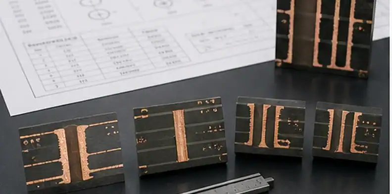
Quick Answer: PCB copper plating thickness should be reviewed as a distribution and hole-wall reliability issue, not only as a nominal copper callout. Buyers should ask where the supplier measures copper, how aspect ratio and panel location affect plating, and what microsection evidence is included for controlled PTH or via reliability.
Key takeaways
- Surface finish thickness and copper plating thickness are different controls.
- Panel edge, dense hole fields, aspect ratio, and copper balance can change plating distribution.
- Microsection evidence is useful when it names the measured hole family and location.
- The RFQ should state which holes or vias are reliability-critical before the supplier prices evidence.
PCB copper plating thickness becomes a real purchasing issue when vias, plated through holes, press-fit holes, or high-current features carry reliability risk. A drawing may state finished copper, but that does not automatically prove that every critical hole wall has enough plating after drilling, desmear, electroless copper, electroplating, and etching.
This article is separate from surface finish thickness requirements, which deals with exposed finishes such as ENIG or other pad coatings. Here the owner is the copper deposited in and around plated holes, especially where distribution makes one area of the panel harder to plate than another.
Table of Contents
- Separate copper plating from surface finish
- Identify the critical hole families
- Review aspect ratio and panel location
- Decide what microsection must show
- Check copper distribution before CAM release
- Compare plating evidence in supplier quotes
- Control changes after first article
- Send QueenEMS the PTH evidence package
Separate copper plating from surface finish
Copper plating thickness belongs to the conductive structure of the board. Surface finish belongs to the exposed soldering, bonding, or contact surface. The two may both appear on a drawing, but they answer different reliability questions. Confusing them can leave a quote with good finish data and weak PTH evidence.
Ask the supplier to separate base copper, plated copper, final copper, hole-wall copper, and surface finish when the build is controlled. Finished outer copper can include base foil plus plating and later process effects. Hole-wall copper needs its own review because it is deposited inside drilled features.
A clean quote should say whether hole-wall copper is built to the customer drawing, IPC class requirement, supplier standard, or a special acceptance plan. Purchasing should not assume that a “2 oz finished copper” note automatically proves every via barrel.
Definition rule: PCB copper plating thickness must identify the copper location before it can control release.
A common example shows the difference: a 1.6 mm board with a 0.20 mm via has a much harder plating path than a large connector hole through the same thickness. The drawing may call both plated holes, but the process margin is not equal.
Finished copper wording can be especially confusing on heavy-copper boards. A buyer may care about outer-layer current capacity, while the reliability concern sits inside a small via barrel. Separate those requirements so a supplier does not answer the easy copper question and miss the hard one.
Identify the critical hole families
Not every hole deserves the same evidence. A tooling hole, nonfunctional via, press-fit connector hole, thermal via array, and high-current plated slot may carry different risk. The RFQ should name the hole families that matter so the supplier can choose sampling and microsection locations intelligently.
The PCB press-fit hole tolerance page is useful when plating thickness and finished-hole size must be reviewed together. Finished hole diameter, plating build, annular ring, and hole quality are tied together. A hole family with tight tolerance may need both dimensional and copper evidence.
| Hole family | Why plating matters | Useful evidence |
|---|---|---|
| Press-fit holes | Insertion stress loads the barrel | Hole size plus wall copper |
| Thermal via arrays | Heat and current depend on continuity | Representative microsection |
| High-current slots | Wall copper carries current | Slot cross-section or coupon |
| Dense blind or small vias | Throwing power may be limited | Family-specific section |
RFQ signal: The supplier can choose better evidence when the buyer names the hole families that cannot fail.
Critical-hole selection also prevents overtesting. A supplier does not need to section every drill size when one small via family, one press-fit hole, and one high-current slot represent the real risk groups.
Also separate plated slots from round holes when they carry current or mechanical load. Slot routing and plating can create different edge coverage than a drilled via, so the evidence plan should name the slot rather than burying it in the drill table.
Review aspect ratio and panel location
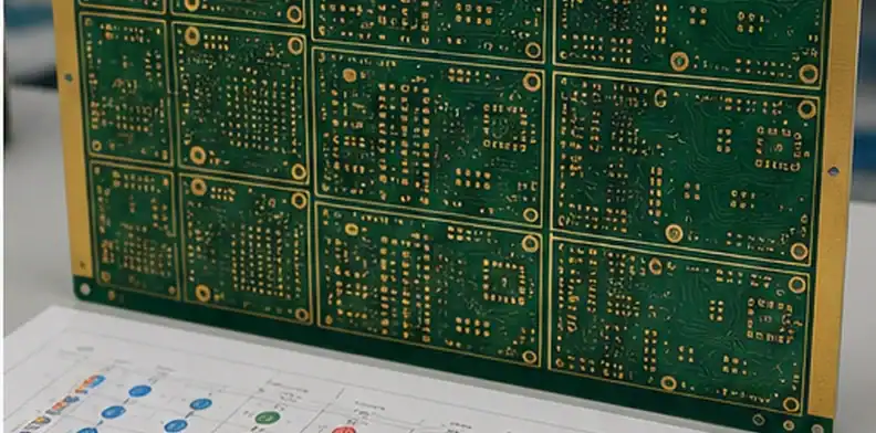
Aspect ratio and panel location affect plating difficulty. A small hole through a thick board is harder to plate evenly than a large hole through a thin board. Dense hole fields and copper-density differences can also change current distribution across the panel.
Ask whether the quoted construction is routine for the supplier’s line or near a process limit. The answer should address the smallest finished hole, board thickness, hole count, panel layout, copper distribution, and any special sampling. A supplier that only repeats “meets IPC” may still be fine, but the buyer has not learned where the margin is.
For controlled work, record whether the sample hole is from the board edge, panel center, dense area, sparse area, or a coupon. Location matters because the easiest feature may not represent the hardest plating condition.
Distribution call: Plating evidence should represent the hardest relevant hole, not only the most convenient coupon.
Aspect-ratio discussion should use the actual board numbers. A 6:1 through hole may be routine for many shops, while an 8:1 or 10:1 small hole can require closer review depending on copper target, drill quality, and line capability.
Panel format can change the answer even when the board data is unchanged. A prototype built on a small panel and a production run built on a larger panel may not share the same plating distribution, coupon placement, or current-density behavior.
Decide what microsection must show
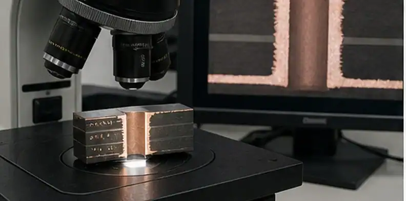
Microsection evidence should show the measured hole or via family, copper thickness at meaningful locations, plating continuity, and any laminate or barrel anomaly. A cross-section photo without a sample map is weaker because the buyer cannot tell whether it represents the critical feature.
Use the PCB microsection report requirements page for report-field detail. For copper plating thickness, add the specific measured family, target requirement, actual reading, magnification or method reference when available, and disposition. The report should make the pass decision easy for quality to understand.
| Microsection field | Buyer use | Common gap |
|---|---|---|
| Hole family | Ties evidence to risk | Only coupon ID is shown |
| Panel location | Shows distribution relevance | Location omitted |
| Minimum reading | Supports acceptance | Only average value listed |
| Disposition | Controls release | No pass/fail owner |
Proof rule: A microsection is release evidence only when the measured feature matches the controlled hole family.
For controlled PTH work, ask whether the report gives minimum wall copper rather than only an average. A 25 um nominal target and a weak low-side reading do not create the same release confidence.
For thick boards, ask whether the reported section shows top, middle, and bottom barrel regions clearly enough to judge throwing power. A single attractive photo can hide a weak center-barrel condition when the report does not state where the minimum reading was taken. When a requirement is customer-driven, attach the customer drawing note or quality clause to the RFQ so the supplier prices the right inspection level from the start.
Check copper distribution before CAM release
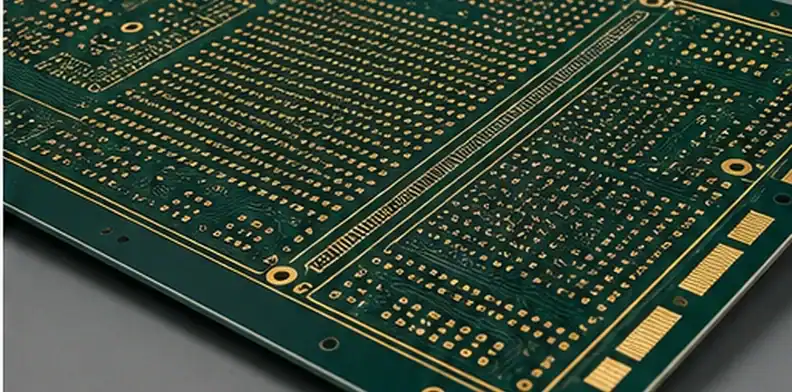
CAM can affect plating distribution through thieving, panel layout, copper balance, hole grouping, and feature density. A supplier may propose copper balancing or panel changes to improve plating, but those changes should be visible before release. Hidden edits can create assembly or electrical side effects.
Link plating review to PCB copper balance drawing review principles without turning the article into a copper-balance duplicate. The question here is not only flatness or etch uniformity; it is whether the panel current distribution and hole placement support the required copper barrel.
Ask the supplier to flag any thieving, panel border, coupon, or layout change that is needed to hold plating thickness. Engineering should approve changes that affect impedance, clearance, keepout zones, or controlled copper areas.
CAM boundary: Plating-support edits are acceptable only when their effect on the released design is visible and approved.
Panel distribution is why coupon location matters. A coupon on a friendly border location may not represent dense via fields near the center of a large production panel.
Copper balancing can improve manufacturability, but it should not invade keepout zones, RF areas, creepage spaces, or controlled thermal reliefs. Ask the supplier to show where thieving or balancing copper is added when the board has sensitive regions.
Compare plating evidence in supplier quotes
Supplier quotes often differ in evidence level. One supplier may include routine electrical test only. Another may include first-lot microsection, coupon location, and hole-wall readings. Those quotes are not technically identical, even when the unit price looks close.
Ask each supplier for the plating assumption, critical hole capability, evidence included, and extra cost or lead time for controlled sampling. That allows purchasing to compare a low-documentation prototype path against a production release path without mixing the two.
| Quote reply | Risk reading | Buyer response |
|---|---|---|
| Includes feature-specific microsection | Strong release record | Review readings against requirement |
| Includes generic coupon only | May miss hard feature | Ask what it represents |
| Electrical test only | Continuity but not wall proof | Decide if enough for the product |
| Extra charge for sectioning | Evidence not in base price | Choose before PO release |
Buyer call: Compare the evidence package, not just the claimed copper class.
Quote comparison should separate continuity evidence from thickness evidence. Electrical test can catch opens, but it cannot show whether a via barrel has enough copper to survive thermal or insertion stress.
A quote that includes sectioning should also name when the sample is taken. First-article sectioning before volume release answers a different question than failure-analysis sectioning after a field issue. Put that timing into the purchase decision.
Control changes after first article
Once a first article is accepted, keep the plating variables stable. A change in drill size, board thickness, panel format, hole count, copper weight, or supplier line can change plating margin. Repeat orders should reference the approved construction and list the changes that need engineering review.
Quality should also know when to ask for renewed evidence. A new panel layout, rush route, alternate material, or yield-driven CAM proposal may justify another microsection or first-lot check. Routine repeats may not need the same report every time if the process and risk remain unchanged.
Keep the approved microsection, drawing revision, stackup, and supplier response together. That record is useful when a future lot shows barrel cracking, intermittent vias, or unexplained assembly failures.
Repeat-order rule: Treat plating evidence as a baseline that must be renewed when the hole or panel condition changes.
Repeat-order review should also watch drill-table edits. A small change from 0.30 mm to 0.25 mm finished hole can alter plating margin even when the board outline and layer count stay the same.
A repeat order should also capture whether the supplier changed from prototype routing to production panelization. That change can alter coupon location and hole-density distribution even when the Gerbers and drill table appear unchanged to purchasing.
Send QueenEMS the PTH evidence package
Send the stackup, board thickness, drill table, finished-hole requirements, via types, copper weights, panel constraints, high-current or press-fit notes, and any required microsection or acceptance standard. QueenEMS can review which hole families need plating evidence and whether the quote should include first-lot cross-section support.
A direct RFQ note is: “PCB copper plating thickness is controlled for the listed PTH and via families. Supplier to state hole-wall copper assumption, representative microsection location, acceptance basis, and approval rule for drill, panel, or copper-weight changes.” Keep that note with the released fabrication data.
Send the drill table and stackup through the QueenEMS contact page when the quotation must separate routine fabrication from controlled PTH evidence.
Handoff rule: The final package should tell the supplier which plated holes carry the reliability risk.
The final package is strongest when it marks the 2 or 3 hole families that need evidence. That narrow request is easier to quote than a vague demand for every plated feature on the board.
For high-current work, include current-carrying holes and slots in the evidence request rather than focusing only on the smallest via. The most difficult geometry and the most critical electrical path are not always the same feature.
FAQ
Is PCB copper plating thickness the same as surface finish thickness?
No. Copper plating thickness controls conductive copper in holes and on copper features, while surface finish thickness controls exposed soldering, contact, or bonding surfaces.
Does electrical test prove enough hole-wall copper?
No. Electrical test proves continuity at the test condition; it does not measure barrel thickness or show plating distribution.
When should I ask for microsection evidence?
Ask for it when small holes, thick boards, high current, press-fit connectors, reliability requirements, or prior failures make hole-wall copper a release concern.
Can panel layout affect plating thickness?
Yes. Panel location, copper density, hole density, and current distribution can change plating uniformity, so representative evidence should match the hard features.
Sources
Written by the QueenEMS Engineering Team
Upload your files today · Free DFM check before production · Ship worldwide
Get your PCB prototypes in as fast as 24 hours. We handle FR4, Rogers, and hybrid boards up to 40 layers in volume production, with advanced builds subject to engineering review — free prototypes for 2–4 layer FR-4 boards, no minimum order.
Just upload your Gerber + BOM — we source every part, assemble, and inspect (AOI + X‑Ray) so you don't have to chase suppliers. Boards ship in as fast as 24 hours.