
Blog
PCB fabrication, PCB assembly, PCB materials, DFM, SMT, HDI, ceramic PCB, and electronics manufacturing guides from QueenEMS.

Centroid File (Pick and Place) PCB Assembly: The Complete Pick and Place Guide
Table of Contents Missing placement data creates a specific engineering question: can the assembler identify each fitted component and its orientation from…

How to Make Your PCB Assembly Transfer Low-Risk
Quick answer: To transfer PCB assembly to a new manufacturer, first confirm which design revision is actually being built. Then give the…

First Article Inspection for PCB Assembly: FAI vs AOI
Quick Answer: First article inspection (FAI) checks whether a representative first build conforms to the released design and agreed production process before…
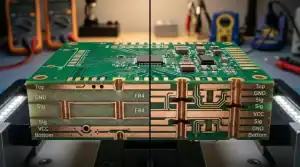
6-Layer vs 8-Layer PCB: Stackups, When to Upgrade, Cost and Lead Time
An 8-layer PCB adds two layers to a 6-layer board, and those two layers are usually spent on an extra ground plane…

PCB Prototype vs Production Order: The 5 Signals That Tell You It’s Time to Switch
Table of Contents You have five perfectly working boards sitting on your desk, and your project manager wants 5,000 units delivered next…

PCB Via Current Capacity: Formula, Worked Examples and Via Count
A standard plated via with a 0.3 mm drill and 20 µm of hole-wall copper has a copper cross-section of about 0.018…
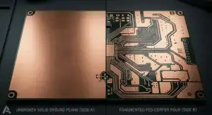
How PCB Copper Pour vs Ground Plane Choices Work
Quick Answer: PCB copper pour vs ground plane decisions should start with return-path continuity, not with how much empty copper looks available…
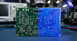
PCB Conformal Coating: Which Type Do You Actually Need — and When Is Skipping It a Mistake?
Table of Contents You review your quote and see an extra line item adding $12 per board for silicone protection, pushing your…
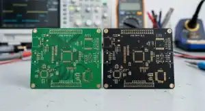
PCB Solder Mask Colors: Cost, DFM and How to Choose
Quick answer: PCB solder mask color is a product and manufacturing choice, not a universal performance grade. Green is commonly offered as…
PCB Design for Test: Test Points, ICT and Flying Probe Checklist
Quick Answer: PCB design for test (DFT) means planning how a bare board and an assembled board will be checked before layout…
IPC Class 2 vs Class 3 PCB: Differences, Standards and Cost
Quick Answer: IPC Class 2 covers products that need continued performance and extended life, where uninterrupted service is desired but is not…
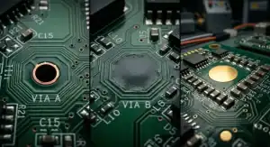
Via Tenting vs Plugging vs Filling: IPC-4761 Types and When to Use Each
Via tenting covers a via with solder mask, plugging pushes material partly into the hole, and filling fills the hole completely, with…