

Quick Answer: You can evaluate PCB assembly quality remote by demanding 8 specific verification data points, including SPI logs, X-ray void percentages (must be under 25%), and First Article Inspection (FAI) reports before authorizing mass production. Approving a 5-board sample run via live video walkthrough prevents up to $40,000 in hidden defect costs. Key takeaways:
- Demand DFM checks upfront to fix design errors before fabrication.
- Request raw AOI defect images instead of simple pass/fail checkboxes.
- Insist on 100% electrical testing like Flying Probe or ICT.
- Identify red flags like blurry pre-shipment photos or refused video tours.
Table of Contents
- 1. What is the Standard PCBA Production Flow?
- 2. Why is Pre-Production DFM Review Your First Gate?
- 3. How to Evaluate SPI Data for Solder Paste Accuracy?
- 4. How to Interpret Remote AOI Reports and Images?
- 5. What Do X-Ray Images Reveal About BGA Joints?
- 6. How Does a First Article Inspection Report Help?
- 7. Why Are Flying Probe and ICT Testing Mandatory?
- 8. How to Implement Pre-Shipment Photo Approval?
- 9. How to Conduct a Live Video Factory Walkthrough?
- 10. What Are the Red Flags of Hidden Quality Issues?
You just wired a 50% deposit to a new offshore EMS partner for your 1,000-unit board run. Now, you sit thousands of miles away, wondering if they actually follow IPC standards or just rush the assembly process. Relying solely on a final shipping notification is a fast track to receiving defective boards you cannot return. You must implement an ironclad system to evaluate PCB assembly quality remote through specific data requests, live visual proof, and strict testing gates before the boards ever leave the factory floor.
1. What is the Standard PCBA Production Flow?
A standard PCBA production flow includes 9 distinct stages from DFM check to final shipping, taking roughly 14 to 21 days for a standard volume order. You must require communication updates at the fabrication, component procurement, assembly, testing, and pre-shipment photo approval stages.
Overcoming the Silent Factory Problem
Buyers frequently complain on the EEVBlog forum that their only communication after ordering is a shipping notification, leaving them completely blind to the production status. You must establish a communication timeline upfront because silence means you cannot evaluate PCB assembly quality remote during active manufacturing.
Here is the truth:
- Demand a notification when bare boards pass bare-board testing.
- Require an update when all components arrive and pass incoming QC.
- Ask for an alert right before the surface mount technology line starts.
- Set a hard stop before the final shipping box is sealed.
Key Takeaway: Bottom line: Set a strict 5-stage communication timeline in your contract so the factory sends production updates instead of just a final tracking number.
| Production Stage | Required Factory Update | Your Remote Action |
|---|---|---|
| Bare Board Fab | AOI pass confirmation | Review layer stackup report |
| Component Sourcing | Shortage/Alternative list | Approve part substitutions |
| Final Assembly | FAI completion alert | Review golden sample photos |
You must halt production at the FAI completion stage to verify the golden sample data before they run the remaining 999 boards.
2. Why is Pre-Production DFM Review Your First Gate?
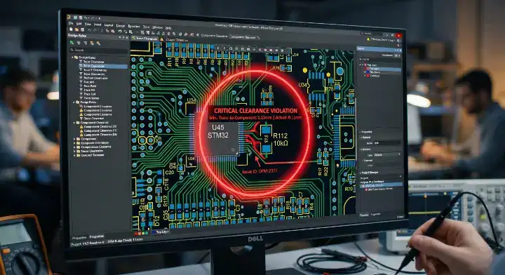
A Design for Manufacturing (DFM) review identifies 80% of footprint and clearance errors before a single board is fabricated. Fixing a trace clearance issue during the DFM stage costs $0, while fixing it after fabrication requires a complete $2,000 board re-spin.
Catching Errors Before Fabrication
Factories often push files straight to the fabrication floor to save time, resulting in short circuits. A proper remote PCB DFM case study shows exactly how factories modify your Gerber files to meet their specific machine tolerances.
Do not ignore these items:
- Verify solder mask expansion values.
- Confirm drill hole sizes match component leads.
- Check copper pour clearances around fine-pitch parts.
Key Takeaway: Bottom line: Demand a formal DFM report PDF and require your signature on it before allowing the factory to cut the first FR4 panel.
| DFM Check Item | Target Metric | Risk if Ignored |
|---|---|---|
| Annular Ring | > 0.1mm | Drill breakout, broken circuits |
| Solder Bridge | > 4 mil clearance | Short circuits during reflow |
| Component Spacing | > 0.25mm | Pick-and-place collision |
Always review the DFM report’s solder bridge clearance values to prevent expensive manual rework after wave soldering.
3. How to Evaluate SPI Data for Solder Paste Accuracy?
Solder Paste Inspection (SPI) is an automated 3D optical check verifying the exact volume, height, and area of paste on every pad, preventing 70% of potential soldering defects. A standard SPI machine measures volume accuracy to within 1%, catching insufficient paste before components are placed.
Reading the SPI Logs
You cannot visually inspect wet solder paste from another continent. You must ask the factory to export the raw SPI data logs to confirm their stencil printing process is stable and repeatable.
Pay close attention to this:
- Look for paste volume standard deviation charts.
- Check the percentage of insufficient paste warnings.
- Review the height data for fine-pitch QFN pads.
Key Takeaway: Bottom line: Request the SPI statistical process control (SPC) chart to prove the factory maintains consistent solder volume across the entire batch.
| SPI Measurement | Acceptable Range | Defect Caused if Out of Bounds |
|---|---|---|
| Paste Volume | 80% – 120% | Open joints or solder bridging |
| Paste Height | ± 15% of stencil | Poor wetting, tombstoning |
| Paste Area | > 85% coverage | Weak mechanical joint strength |
If the SPI paste volume drops below 80% on specific pads, instruct the factory to clean their stencil immediately.
4. How to Interpret Remote AOI Reports and Images?

Automated Optical Inspection (AOI) scans identify 90% of surface defects, capturing component misalignments down to 01005 package sizes. A proper remote AOI report includes high-resolution defect images and statistical yield trends, rather than simple summary statements.
Rejecting Pass/Fail Checkmarks
Buyers frequently complain on Electronics Stack Exchange that their PCB QC report sample features only pass/fail checkmarks without actual inspection data. This leaves you completely unable to verify if the factory actually performed the test or just rubber-stamped the paperwork.
Look at the real numbers:
- Demand raw statistical data for false calls.
- Require minimum 8 specific data points per board.
- Insist on high-resolution defect images for any flagged part.
- Verify polarity marks on all diodes and ICs in the photos.
Key Takeaway: Bottom line: Never accept a summary checkbox; demand the raw AOI defect images to evaluate PCB assembly quality remote accurately.
| AOI Data Point | What it Verifies | Action if Failed |
|---|---|---|
| XY Offset | Placement accuracy | Calibrate pick-and-place head |
| Polarity Check | IC orientation | Manually rework component |
| Solder Fillet | Wetting quality | Adjust reflow oven profile |
Always correlate the offset measurements in the AOI report with your acceptable footprint tolerances.
5. What Do X-Ray Images Reveal About BGA Joints?
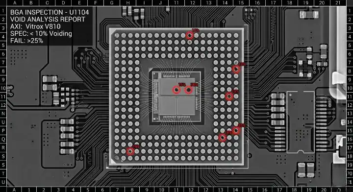
X-Ray inspection uses high-frequency electromagnetic radiation to penetrate component packages and reveal hidden solder spheres underneath BGA and QFN chips. IPC-A-610 standards mandate that total voiding within a single BGA solder ball must remain below 25% of the total ball area.
Analyzing the Void Percentages
You cannot inspect a BGA visually because the pins are entirely underneath the plastic package. A detailed X-ray inspection guide proves that requiring specific voiding calculations prevents components from detaching in the field.
Make no mistake:
- Check the report for exact voiding percentage numbers.
- Look for short circuits between adjacent hidden balls.
- Identify head-in-pillow defects caused by poor reflow.
Key Takeaway: Bottom line: Demand 3D X-ray images with overlay measurement circles showing the exact voiding percentage for every BGA component.
| X-Ray Finding | IPC-A-610 Limit | Impact on Quality |
|---|---|---|
| Solder Voiding | < 25% area | Weakens mechanical strength |
| Bridging | Zero allowed | Immediate electrical short |
| Head-in-Pillow | Zero allowed | Intermittent electrical failure |
If the X-ray report shows 30% voiding, reject the board and force the factory to adjust their thermal profile.
6. How Does a First Article Inspection Report Help?
First Article Inspection (FAI) is the rigorous verification of the very first board off the assembly line against the original BOM and design files. Approving a 5-board FAI sample run prevents mass production errors, saving hardware startups an average of $20,000 in batch rework costs.
Setting the Golden Standard
You must review the first article inspection data carefully because it sets the acceptable quality limit for the rest of the order. At QueenEMS, we freeze mass production until the client reviews the FAI top/bottom photos and gives explicit written approval.
Pay close attention to this:
- Cross-reference the FAI component markings with your BOM.
- Verify the physical PCB thickness and color.
- Check the conformal coating boundaries visually.
Key Takeaway: Bottom line: Halt all production and demand high-resolution photos of the First Article board to verify exact component placement before continuing.
| FAI Checklist Item | Verification Method | Buyer Action |
|---|---|---|
| Component Values | Read top markings in photos | Compare directly to BOM |
| Solder Quality | Review AOI images | Approve wetting angles |
| PCB Dimensions | Caliper measurement photo | Verify enclosure fit |
Use the FAI component marking photos to confirm the factory did not use cheaper substitute parts without permission.
7. Why Are Flying Probe and ICT Testing Mandatory?
Flying probe testing uses robotic arms to measure resistance, capacitance, and open/short circuits on individual nets without requiring a custom fixture. ICT (In-Circuit Testing) uses a custom “bed of nails” to test up to 1,000 nodes simultaneously, processing complex boards in under 30 seconds.
Validating Electrical Integrity
Visual inspections like AOI cannot tell you if a capacitor value is correct or if a trace is broken internally. Implementing proper functional testing strategies forces the factory to prove the board carries current exactly as designed.
Consider this reality:
- Demand the flying probe test log file.
- Request the exact test coverage percentage.
- Ask for the raw data on any failed nets.
Key Takeaway: Bottom line: Require a 100% electrical test pass rate on your purchase order to evaluate PCB assembly quality remote effectively.
| Testing Method | Setup Cost | Ideal Production Volume |
|---|---|---|
| Flying Probe | $0 (No fixture) | Prototypes (<500 units) |
| ICT | $2,000+ (Custom fixture) | Mass Volume (>5,000 units) |
| Functional Test | Varies by jig | All volumes |
Review the flying probe coverage report to identify which nets the machine physically could not reach.
8. How to Implement Pre-Shipment Photo Approval?
Pre-shipment photo approval is a contractual hold point where the factory sends high-resolution images of the packed boxes and finished boards before handing them to FedEx. This simple step requires zero extra equipment and prevents factories from shipping severely damaged or incomplete batches.
Protecting Against the “We Inspected It” Excuse
Buyers often face dispute scenarios where they receive damaged boards, but the factory claims “we inspected everything before shipping.” You must build a pre-shipment approval process requiring visual proof of the finished lot to protect yourself from these liability shifts.
Here is the truth:
- Demand photos of the boards sealed in anti-static bags.
- Require a picture of the external shipping box with labels.
- Ask for a photo of the completed functional test jig screen.
Key Takeaway: Bottom line: Withhold the final 50% payment until the factory provides clear, high-resolution pre-shipment photos of your exact order.
| Photo Requirement | What It Proves | Dispute Prevention |
|---|---|---|
| Anti-static bags | Proper ESD handling | Rejects static damage claims |
| Serial numbers | Traceability intact | Proves the specific batch size |
| Packing material | Adequate drop protection | Shifts shipping damage liability |
Always cross-check the serial numbers in the pre-shipment photos with your final invoice quantities.
9. How to Conduct a Live Video Factory Walkthrough?
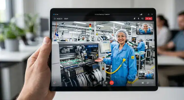
A live video factory walkthrough is a real-time Zoom or WeChat call where the project manager shows your specific boards moving down the SMT line. This 15-minute call provides more authentic quality verification than a dozen staged marketing photos.
Directing the Camera
You must control the video call by asking the operator to point the camera at specific machines rather than letting them show only the conference room. Ask them to zoom in on the feeder reels to verify component brands.
Do not ignore these items:
- Ask to see the calibration stickers on the ovens.
- Request a live view of the AOI operator’s monitor.
- Demand to see the scrap bin to gauge their defect volume.
Key Takeaway: Bottom line: Schedule an unannounced 10-minute video call during your production window to verify they are actually using the automated equipment promised.
| Walkthrough Request | What to Look For | Factory Implication |
|---|---|---|
| Component Reels | Original brand labels | Prevents counterfeit parts |
| SMT Line Speed | Smooth, continuous flow | Indicates well-maintained machines |
| Worker ESD Gear | Wrist straps plugged in | Proves strict ESD compliance |
Use the video call to confirm the operators are actually wearing grounded ESD wrist straps while handling your boards.
10. What Are the Red Flags of Hidden Quality Issues?
A major quality red flag is a factory refusing to provide raw X-ray or SPI data files, citing “internal company policy.” Transparent manufacturers share their machine logs willingly because accurate data proves their high manufacturing standards.
Spotting the Warning Signs
When a factory takes 48 hours to provide a single photo of a completed board, it means they are manually reworking a massive defect issue behind your back. At QueenEMS, we provide 3D AOI and X-Ray inspection on every BGA joint and share the exact data immediately.
Make no mistake:
- Refusing a live video tour indicates outsourced production.
- Sending blurry partial photos hides bad soldering.
- Missing lot traceability numbers prevents future recall management.
Key Takeaway: Bottom line: Cancel the mass production transition immediately if the factory provides blurry photos or refuses to share the raw AOI defect logs.
| Red Flag Behavior | Hidden Factory Problem | Your Required Action |
|---|---|---|
| Blurry QC photos | Hiding cold solder joints | Demand 4K macro images |
| Missing X-ray data | BGA voiding out of spec | Halt payment immediately |
| Refused video call | Order was subcontracted out | Audit their facility physically |
Always demand high-resolution images because blurry photos are intentionally used to mask severe solder bridging.
Frequently Asked Questions (FAQ)
Can I hire a third-party inspector to check my boards in China? Yes, hiring a third-party inspection company costs between $200 and $400 per day. They visit the factory, perform visual IPC-A-610 checks, verify quantities, and send you an independent report before shipping. Book the inspector directly to maintain unbiased oversight.
What’s the best way to verify if they used genuine components? Demand a traceably sourced component purchase record and clear photos of the component reels. Counterfeit parts often have inconsistent laser markings or missing moisture-sensitive labels. Always require them to source critical ICs directly from authorized distributors like Digi-Key or Mouser.
How do I know if the factory actually performed the flying probe test? Request the machine-generated raw test log file, which includes time stamps and specific net names. A real log file cannot be easily faked and will show exact resistance measurements for every connection on the board. Never accept an Excel sheet with just the word “Passed.”
What should I do if the pre-shipment photos show defects? Halt the shipment immediately and circle the exact defects in the photos. Send the marked images back to the project manager and demand a formal 8D corrective action report detailing how they will rework the boards and prevent the issue in the future.
We know how stressful it is to manage hardware manufacturing from another continent. Blind trust leads to broken products, which is why transparent data is your only real defense. At QueenEMS, we offer a Free DFM/DFA engineering review on every order and guarantee a 24-hour fastest turnaround for critical prototypes.
Stop guessing about your offshore manufacturing quality. Demand transparent data, verifiable testing, and live communication for every batch. Contact us at QueenEMS today to experience a truly transparent PCB assembly partnership.
Written by the QueenEMS Engineering Team
Upload your files today · Free DFM check before production · Ship worldwide
Get your PCB prototypes in as fast as 24 hours. We handle FR4, Rogers, and Flex up to 60 layers — free prototypes for 2–4 layer boards, no minimum order.
Just upload your Gerber + BOM — we source every part, assemble, and inspect (AOI + X‑Ray) so you don't have to chase suppliers. Boards ship in as fast as 24 hours.