

Quick Answer: A structured NPI PCB assembly process typically spans 6 to 10 weeks and systematically prevents 80% of volume manufacturing failures. Executing pilot runs and early DFM reviews directly saves an average of $28,000 in late-stage re-spin costs. Key takeaways:
- Working prototypes fail 44% of the time in production without proper validation.
- Missing centroid data delays manufacturing timelines by 4 to 8 weeks.
- SMT pilot runs require exact batch sizes of 10 to 50 units for statistical validity.
- Formal gate reviews separate real EMS partners from high-volume “copy-exact” factories.
Table of Contents
- 1. What Is the 6-Stage Process for NPI PCB Assembly?
- 2. What Files Must You Prepare Before Manufacturing Begins?
- 3. Why Are Pilot Runs Critical for PCBA Scale-Up?
- 4. How Does Early DFM Accelerate Your Product Launch?
- 5. Who Handles What During the NPI Execution Phase?
- 6. What Are the Top Failure Modes When Scaling to Volume?
- 7. How Should Your Contract Manufacturer Supervise the Build?
- 8. What Data Belongs in a Valid Engineering Sign-Off Report?
- 9. Is Your Factory Faking Their NPI Process?
- 10. How Long Does the Transition to Mass Production Actually Take?
You just finished testing a working prototype on your bench, and it functions perfectly. The next logical step seems to be ordering a 1,000-unit volume run to hit your market launch deadline. Two weeks later, the factory calls to inform you that 30% of the boards suffer from BGA shorts, and five components are End-of-Life (EOL), causing a massive delay. This nightmare happens because a working prototype is fundamentally different from a production-ready design, which is why you need a strict NPI PCB assembly framework.
1. What Is the 6-Stage Process for NPI PCB Assembly?
The 6-stage process for NPI PCB assembly spans Define, Feasibility, Development, Pilot Production, Evaluation, and Full Production to eliminate 44% of early-stage manufacturing errors. This structured gateway system guarantees that no product advances to volume manufacturing until all design constraints pass strict verification.
How do the first three stages work?
The first half of the process locks down the design variables before any physical boards are printed. During the Define and Feasibility stages, engineers review the schematic against supply chain realities to flag EOL components immediately. This early filtering dictates the entire project budget and lead time.
Consider the reality:
- The Define phase solidifies product specifications and regulatory requirements.
- Feasibility tests whether the target price aligns with the required Bill of Materials.
- Development forces a strict DFM review to adjust footprints for automated assembly.
What happens during pilot and evaluation?
The final three stages transition the verified data into physical hardware. Pilot Production physically tests the SMT lines with a tiny batch to expose hidden thermal issues. Evaluation documents every defect found during the pilot, generating a formal engineering report.
Bottom line: Never authorize Full Production until the Evaluation stage generates a signed engineering report proving the pilot run achieved a high yield.
| NPI Stage | Core Activity | Critical Deliverable |
|---|---|---|
| Feasibility | BOM supply chain check | Cost and lead time estimate |
| Development | DFM and DFA engineering | Adjusted CAD and Gerber files |
| Pilot | Small physical batch run | Thermal profiles and machine setup |
| Evaluation | Yield and defect analysis | Formal NPI sign-off report |
Data shows that failing to complete the Development stage before Pilot Production increases defect rates by 35%.
2. What Files Must You Prepare Before Manufacturing Begins?

OEMs must provide an 8-10 item readiness checklist before starting NPI PCB assembly, because missing centroid data or EOL components causes 4-8 weeks of delays. A contract manufacturer cannot guess your component orientations, which means incomplete data packages force the line to stop.
Which files cause the longest production delays?
A centroid file is a spatial coordinate document mapping the exact X-Y position and rotation of every component. Missing or mismatched centroid files represent the number one cause of pre-production delays. When this file contradicts the Gerber data, machines place parts backward, resulting in catastrophic functional failures.
Many clients send mismatched CAD data, which means production stalls indefinitely. At QueenEMS, we run a mandatory Free DFM/DFA engineering review on every centroid file upon receipt. This verification step catches 100% of placement errors before physical manufacturing begins.
What are the 4 critical pre-build checks?
Factories execute 4 specific pre-build checks before ordering a single bare board. These checks include BOM scrubbing for obsolete parts, stencil verification for paste release, build pack documentation audits, and CAD data alignment.
Here is what you need to provide:
- Native CAD files (Altium, Eagle, or KiCad).
- Exported Gerber RS-274X or ODB++ files.
- A clean Excel BOM with manufacturer part numbers.
- Detailed assembly drawings indicating specific test points.
Bottom line: Submit an ODB++ file format instead of standard Gerbers, because it inherently includes netlists and centroid data in one package, preventing file mismatch errors entirely.
| Missing Document | Manufacturing Consequence | Average Delay Time |
|---|---|---|
| Centroid Data | Pick-and-place programming fails | 3 to 5 days |
| Assembly Drawings | Polarity and orientation errors | 1 to 2 weeks |
| Specific MPNs | Purchasing buys wrong footprint | 4 to 8 weeks |
Auditing these four pre-build documents drops technical query hold-ups by over 80%.
3. Why Are Pilot Runs Critical for PCBA Scale-Up?
Skipping pilot runs in NPI PCB assembly costs OEMs an average of $28,000 per late-stage re-spin, because a working bench prototype is fundamentally not a production-ready design. A hand-soldered board proves the electronic theory, but a machine-assembled board proves the manufacturing capability.
Why is a working prototype not enough?
A working prototype built in a lab bypasses the thermal dynamics of a 10-zone reflow oven. Hand-soldering covers up poor pad designs that will inevitably cause tombstoning when subjected to automated surface mount technology. The pilot run exists specifically to break the process and find these weak points.
Hardware startups routinely underestimate the leap from prototype to production by a factor of three. Without a pilot validation, you are gambling your entire component inventory on a single, untested machine program.
What is the ideal pilot run batch size?
A standard pilot run size is an exact batch of 10 to 50 units. Producing fewer than 10 units fails to generate enough statistical variance to calculate SMT yield rates. Producing more than 50 units risks wasting expensive components if a major footprint error exists.
Why does this specific range matter?
- It provides enough boards for destructive testing.
- It allows engineers to dial in the solder paste printer.
- It exposes systemic issues without draining your budget.
Bottom line: Always mandate a 50-unit pilot run for any board containing BGAs or fine-pitch QFNs to verify stencil aperture accuracy before volume scale-up.
| Build Type | Purpose | Risk Level if Skipped |
|---|---|---|
| Bench Prototype | Verify electronic function | N/A (Starting point) |
| Pilot Run (10-50) | Verify machine yield | Critical ($28k average loss) |
| Volume Run | Meet market demand | Catastrophic |
Data proves that executing a 50-unit pilot run slashes volume production failure rates from 44% down to under 2%.
4. How Does Early DFM Accelerate Your Product Launch?
Involving your CM for DFM review before design freeze during the NPI PCB assembly process cuts your timeline by 4 weeks, resulting in 10x lower engineering change costs. Late-stage design changes require halting the line, re-ordering bare boards, and buying new stencils.
When should you initiate DFM reviews?
The ideal time to initiate Design for Manufacturing (DFM) is right after your schematic is locked but before you route the final PCB traces. At this moment, adjusting a footprint to match factory stencil requirements costs zero dollars. Waiting until the gerbers are generated means any correction requires a full engineering change notice (ECN).
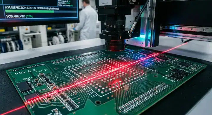
Customers often submit boards with inadequate BGA escape routing, which means hidden shorts occur during reflow. We mandate a Free DFM/DFA engineering review and use 3D AOI + X-Ray inspection on every BGA joint. This proactive intervention guarantees a 99.7% first-pass yield on complex builds.
What makes early involvement critical?
Early CM involvement allows the factory purchasing team to secure long-lead-time components while you finish the layout. If you wait until the design freeze to check the BOM, you might discover your main microcontroller has a 52-week lead time.
Here are the direct benefits of early engagement:
- Stencil thickness gets matched to the most difficult component.
- Panelization strategies are optimized to save material costs.
- Test points are added to the bottom layer for bed-of-nails access.
Bottom line: Send your preliminary BOM to your factory 30 days before your design freeze to identify supply chain bottlenecks while you still have time to redesign.
| Involvement Timing | Engineering Change Cost | Timeline Impact |
|---|---|---|
| Before Design Freeze | $0 (Software edit) | None |
| After Prototype | $2,000+ (New tooling) | +2 weeks |
| During Volume Run | $28,000+ (Scrap inventory) | +8 weeks |
Engaging your CM before design freeze is the single most effective action to prevent cost overruns.
5. Who Handles What During the NPI Execution Phase?
Responsibility during NPI PCB assembly is strictly divided, where OEMs supply verified CAD files and the CM executes the 7 specific execution steps including batch sizing and documentation. Blurring these lines leads to finger-pointing when a batch fails electrical testing.
What are the CM’s exact responsibilities?
The factory assumes total responsibility for translating your digital files into physical machine instructions. This includes designing the solder paste stencil, writing the pick-and-place machine programs, and establishing the thermal reflow profile. The CM must also procure the exact components listed unless an alternative is explicitly approved.
OEMs, conversely, must deliver a flawless data package. If you provide an assembly drawing with ambiguous polarity markings for a diode, the resulting failure is your responsibility. Clarity in documentation is your primary duty.
How do the 7 execution steps flow?
The execution phase follows a rigid, non-negotiable sequence. It begins with establishing the pilot batch size and ends with the formal status change to mass production.
The sequence unfolds like this:
- Batch sizing determines the material draw.
- Machine programming translates the centroid data.
- Assembly supervision monitors the first board out.
- The sign-off gate reviews the yield metrics.
Bottom line: Demand a formal responsibility matrix contract from your CM to legally dictate who pays for scrapped boards if a machine placement error occurs.
| Responsibility | OEM Duty | CM Duty |
|---|---|---|
| Data Integrity | Provide clean Gerbers and BOM | Verify files match machine limits |
| Machine Setup | Answer technical queries quickly | Create thermal and placement profiles |
| Quality Control | Define functional test parameters | Execute AOI, X-Ray, and generate report |
A clear division of labor prevents the miscommunications that typically cause 2-week production halts.
6. What Are the Top Failure Modes When Scaling to Volume?
The leading failure modes in NPI PCB assembly include mismatched centroid files, EOL components, and incorrect stencil aperture ratios which cause insufficient solder on 30% of boards. Understanding these root causes allows hardware teams to design preventative measures directly into the CAD package.
How do BOM and footprint errors happen?
Footprint mismatch is a failure mode where the physical component is larger or smaller than the copper pads drawn on the PCB. This occurs because engineers rely on unverified third-party CAD libraries instead of reading the manufacturer’s datasheet. This error mandates a total board re-spin.
Another frequent failure mode is the inclusion of obsolete parts in the BOM. Startups often design around components they bought from a distributor two years ago, ignoring product lifecycles. When the CM tries to buy reels, the parts no longer exist.
Why do stencil and solder defects occur?
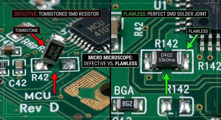
Solder defects like tombstoning happen when unequal thermal mass causes one end of a passive component to melt faster than the other. This pulls the resistor upright like a tombstone, severing the connection. Poor stencil aperture design directly causes bridging between fine-pitch IC pins.
Consider these common defect triggers:
- Vias placed directly inside component pads siphon solder away.
- Heavy copper planes without thermal reliefs cause cold joints.
- Applying too much paste pressure causes BGA shorts.
Bottom line: Apply thermal reliefs to all ground plane connections in your CAD software to guarantee uniform heat distribution and prevent cold solder joints.
| Failure Mode | Root Cause | Prevention Method |
|---|---|---|
| Tombstoning | Unequal thermal mass on pads | Implement strict pad size parity |
| Component Obsolete | Using outdated CAD libraries | Check lifecycle status via API |
| BGA Bridging | Incorrect stencil thickness | Factory calculates area ratio |
Correcting footprint dimensions before the pilot run saves OEMs thousands of dollars in wasted stencil fees.
7. How Should Your Contract Manufacturer Supervise the Build?
Dedicated engineers supervise every NPI PCB assembly build by monitoring machine setups, verifying SMT pick-and-place accuracy, and locking down thermal profiles to prevent defects. High-volume factories running “copy-exact” models fail here because they refuse to slow down their lines for intensive observation.
Why is engineering supervision mandatory?
An NPI build is an experiment, which means things will inevitably go wrong. A dedicated engineer stands at the end of the SMT line to inspect the first article immediately. If the solder paste printer is misaligned by 50 microns, the engineer halts the line before 49 more defective boards are printed.
Some startups receive boards with hidden BGA voids because the CM skipped thermal profiling. We assign a dedicated engineer to execute thermal tracking on every build, even our Free 2-4 layer FR4 prototypes. This intensive oversight eliminates field returns for early-stage hardware companies.
How do they control the execution steps?
The supervision process relies on strict First Article Inspection (FAI). The engineer uses Automated Optical Inspection (AOI) to compare the first assembled board against the digital CAD model. Every single component is checked for presence, polarity, and acceptable solder fillets.
Key supervision checkpoints include:
- Solder paste volume measurement via 3D SPI.
- Reflow oven zone temperature calibration.
- X-ray inspection of all bottom-terminated components.
Bottom line: Ask your CM for the name of the specific engineer assigned to supervise your pilot run; if they cannot provide one, they are treating your project like a generic volume order.
| Supervision Task | Technology Used | Defect Prevented |
|---|---|---|
| Paste Verification | 3D Solder Paste Inspection | Insufficient solder joints |
| Placement Check | Automated Optical Inspection | Polarity/Missing parts |
| Hidden Joint Check | 2D/3D X-Ray | BGA voids and shorts |
Dedicated engineering oversight catches 98% of machine calibration errors on the very first board.
8. What Data Belongs in a Valid Engineering Sign-Off Report?
A valid NPI PCB assembly report must contain build details, process flow documentation, specific defect images, and DFM recommendations to authorize the volume build. This document is the ultimate deliverable of the pilot phase, serving as your objective proof of manufacturing readiness.
What critical sections must the report include?
The report begins with a high-level summary of the yield metrics, stating exactly how many boards passed and failed. It must include a detailed process flow section documenting the exact machine parameters, reflow profiles, and stencil thicknesses used. This creates a reproducible baseline for future volume runs.
Crucially, the report must contain high-resolution images of every defect encountered. If a QFN chip experienced voiding, the X-ray image must be attached alongside a root cause analysis. Without this data, you cannot update your design files accurately.
How does the sign-off process work?
The sign-off is a formal gateway where the OEM and CM agree the product is ready. The CM provides actionable recommendations, such as suggesting a slight pad reduction to stop solder bridging. The OEM then updates the CAD files and officially changes the project status to “Production.”
What the sign-off requires:
- Approval of all alternative component substitutions.
- Acknowledgment of acceptable yield thresholds.
- Verification of test fixture functionality.
Bottom line: Refuse to pay the final NPI invoice until the factory delivers a comprehensive engineering report containing specific DFM layout recommendations for your next revision.
| Report Section | Critical Data Point | Action Required |
|---|---|---|
| Yield Summary | Pass/Fail percentage | Determine if re-spin needed |
| Defect Log | X-ray images of failures | Update PCB layout files |
| Process Baseline | Reflow thermal profile | Lock parameters for volume |
A formal NPI report transitions institutional knowledge from the engineering team directly to the mass production floor.
9. Is Your Factory Faking Their NPI Process?
You can expose a fake NPI PCB assembly process by asking 5 specific evaluation questions, because fake CMs use high-volume “copy-exact” methods without assigning dedicated engineers. Many contract manufacturers claim to offer NPI, but they simply throw your files onto a standard SMT line and ship whatever comes out.
What are the red flags of a fake process?
The biggest red flag is a factory that demands perfect files from day one and provides zero DFM feedback. A real NPI partner expects your design to have flaws and actively hunts for them. If a CM accepts a complex 12-layer board design and pushes it to production in 48 hours without asking a single technical question, they are bypassing NPI entirely.
Another massive red flag is the absence of a dedicated gate review. If the factory transitions from a 20-unit prototype directly into a 5,000-unit run without holding a formal meeting to discuss yield issues, you are working with a vendor, not an engineering partner.
Which 5 evaluation questions should you ask?
To test their capabilities, ask targeted questions about their failure resolution protocols. Real factories have structured answers; fake ones offer vague reassurances.
Ask these exact questions:
- Do you assign a dedicated engineer to physically supervise the pilot run?
- Will you provide a formal NPI report with X-ray images before volume production?
- What is your standard procedure when the centroid file mismatches the Gerber?
- Do you generate a custom reflow profile for every new board?
- At what specific gate do we officially transition to mass production?
Bottom line: If a contract manufacturer cannot produce a sanitized NPI report from a previous client as an example of their workflow, walk away immediately.
| Factory Type | Engineering Support | Defect Handling |
|---|---|---|
| True NPI Partner | Dedicated assigned engineer | Halts line, issues DFM report |
| Fake CM (“Copy-Exact”) | None (Standard operators) | Ships defective boards, blames OEM |
Asking these five technical questions filters out 90% of low-tier manufacturers masquerading as engineering partners.
10. How Long Does the Transition to Mass Production Actually Take?
A medium-complexity NPI PCB assembly project takes exactly 6 to 10 weeks to complete, which means transitioning to full volume production requires precise timeline management. Founders consistently underestimate this window, assuming a 5-day quick-turn prototype translates to a 5-day production setup.
How do you estimate realistic timelines?
The timeline is dictated by component procurement and bare board fabrication complexity. A simple 2-layer board with standard parts takes 4 weeks. However, a complex 8-layer HDI board with specialized BGAs requires 8 to 12 weeks. Procurement alone consumes 60% of this timeframe.
You must account for the gate reviews. It takes 3 days to analyze the pilot run results, and another week for your team to implement the DFM feedback into the CAD files. These iterations cannot be rushed without severe risk.
How does the transition to volume production happen?
Once the NPI report is signed off, the status officially changes. The CM locks the machine programs and orders components in bulk reels. The transition marks the moment engineering hands control over to the production management team.
Key transition milestones:
- Tooling and stencils are permanently archived.
- Standard Operating Procedures (SOPs) are finalized for operators.
- Automated testing fixtures are locked down for high throughput.
Bottom line: Build an 8-week buffer into your market launch schedule strictly for the NPI iteration phase to prevent missing critical delivery deadlines.
| Board Complexity | Definition | Realistic NPI Timeline |
|---|---|---|
| Simple | 2-4 layers, common passive parts | 4 to 6 weeks |
| Medium | 6-8 layers, standard BGAs/QFNs | 6 to 10 weeks |
| Complex | 10+ layers, HDI, blind/buried vias | 10 to 14 weeks |
Accurate timeline estimation prevents the panicked, expedited shipping fees that destroy hardware profit margins.
Skipping the critical NPI steps turns minor CAD oversights into $28,000 disasters. By demanding formal DFM reviews, executing strict 50-unit pilot runs, and requiring signed engineering reports, you effectively eliminate 80% of volume manufacturing failures. A true manufacturing partner does not just print your files; they actively engineer the risk out of your product. QueenEMS stands behind this philosophy with our 24-hour engineering reviews, advanced 3D X-ray capabilities, and up to 60-layer fabrication capacity. Stop gambling your production budget on unverified prototypes—contact us today to build a flawless NPI strategy.
FAQ
Can I skip the NPI phase if my prototype works perfectly? No, you cannot safely skip it because a lab prototype does not prove machine manufacturability. Bench testing verifies electronic theory, but NPI proves the board can survive automated reflow ovens without defects.
What is the best batch size for a pilot run? The best size is exactly 10 to 50 units. This specific range provides enough statistical data to calculate accurate SMT yield rates without wasting expensive components on a flawed design.
How do I know if my centroid file is ready for manufacturing? Yes, it is ready if it precisely matches the X-Y coordinates and rotation data of your final Gerber pads. Submitting an ODB++ file format automatically guarantees this alignment and prevents 4-8 weeks of delays.
Does early DFM review actually save money? Yes, early DFM saves thousands of dollars because changing a footprint in CAD costs nothing. Waiting until the pilot run fails forces you to scrap physical inventory, averaging $28,000 in re-spin costs.
What should I do if my CM doesn’t provide an NPI report? You must halt volume production immediately because this indicates a fake, “copy-exact” process. Demand a formal gate review with X-ray images of your BGA joints before authorizing mass manufacturing.
Upload your files today · Free DFM check before production · Ship worldwide
Get your PCB prototypes in as fast as 24 hours. We handle FR4, Rogers, and Flex up to 60 layers — free prototypes for 2–4 layer boards, no minimum order.
Just upload your Gerber + BOM — we source every part, assemble, and inspect (AOI + X‑Ray) so you don't have to chase suppliers. Boards ship in as fast as 24 hours.