
Blog
PCB fabrication, PCB assembly, PCB materials, DFM, SMT, HDI, ceramic PCB, and electronics manufacturing guides from QueenEMS.
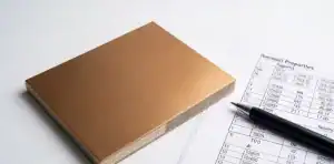
How to Qualify Isola 370HR PCB material
Isola 370HR PCB material: interpret Tg, T288 and Df, screen equivalents, set approval gates, and prepare a controlled fabrication RFQ….
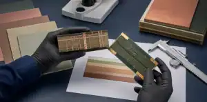
How to Specify IT-150DA PCB material Correctly
Evaluate IT-150DA PCB material using current datasheet conditions, buildable stack-ups, fabrication controls, and a controlled RFQ package….
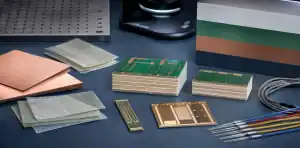
How to qualify IT-140 PCB material for production
Assess IT-140 PCB material with REV 2.0-17 data, assembly-profile evidence, controlled substitutions, and a complete RFQ package….
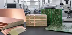
How to Qualify KB-6160 for Standard FR-4 PCBs
Qualify KB-6160 using construction-specific Dk/Df, current supplier evidence, stack-up controls, thermal requirements, and PCB test records….
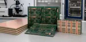
What Makes VT-47 a Reliable High-Tg PCB Material?
Specify VT-47 with verified thermal data, construction-specific Dk/Df, process controls, supplier evidence, and PCB qualification tests….
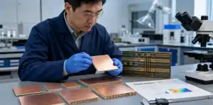
How to Evaluate NP-170 Beyond Its Tg Rating
Use this NP-170 guide to verify the exact Nanya grade, thermal margin, stack-up, process controls, substitutions, and RFQ evidence….
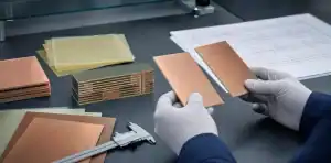
How to Specify NP-150 Without Material Ambiguity
Use this NP-150 guide to confirm the full Nanya grade, thermal data, stack-up, processing controls, and RFQ evidence before PCB production….
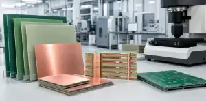
How to Evaluate NP-140 for Reliable PCB Builds
Evaluate NP-140 properties, sourcing evidence, processing questions, and upgrade signals before approving it for an FR-4 PCB stack-up….
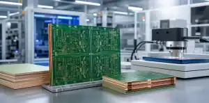
How to Choose TU-662 for Reliable PCB Production
Compare TU-662 and TU-662F specs, applications, and upgrade signals for cost-driven PCB production….
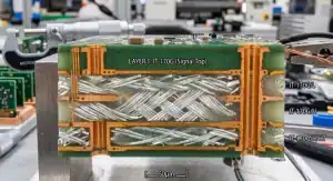
How to Choose Between IT-150DA and S1150G for Halogen-Free PCBs
IT-150DA represents a critical pivot point in PCB manufacturing, acting as the bridge where engineers finally abandon low-tier Tg130 materials in favor…
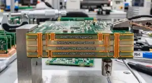
How to Choose the Right IT-170 PCB Material Variant
IT-170 is a mid-tier Tg170 FR-4 laminate family engineered by ITEQ to bridge the gap between standard thermal performance and advanced signal…
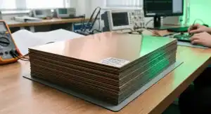
How To Choose Between S1170G and S1000-2M for Multi-Layer PCBs
Procurement teams constantly struggle to balance strict environmental compliance against skyrocketing material costs when designing high-temperature multi-layer boards. For years, engineers blindly…