

Quick Answer: PCB manufacturing steps convert released design data into a bare circuit board through CAM preparation, imaging, etching, lamination where required, drilling, copper deposition, outer-layer patterning, protective coatings, pad finishing, depaneling, net testing, and shipment inspection. The exact route changes with layer count and special features, so a buyer should approve the files, stack-up, material, finish, test method, and any CAM changes before production. PCB assembly begins only after the bare board passes these fabrication controls.
Understanding the route helps you control more than schedule. Each operation can preserve the design intent, introduce an allowed manufacturing compensation, or create a defect that becomes hidden by the next operation. A useful process review therefore asks what goes in, what can change, what evidence comes out, and who may release the next stage.
This article follows a conventional rigid bare-board route. Single-sided boards skip multilayer operations, while HDI, rigid-flex, heavy-copper, controlled-depth, or sequential-lamination constructions add their own steps. The goal is not to memorize a factory tour. It is to know where a drawing, stack-up, CAM question, coupon, or inspection record belongs in the purchase decision.
Table of Contents
- Files and approvals before fabrication starts
- Inner-layer imaging and copper etching
- AOI, oxide treatment, and multilayer lay-up
- Lamination turns separate layers into one board
- Drilling and hole-wall preparation
- Copper deposition and outer-layer patterning
- Solder mask, legend, and surface finish
- Profiling, routing, and panel separation
- Electrical test and final inspection
- Build an RFQ around the manufacturing route
Files and approvals before fabrication starts
The route through pcb manufacturing steps should start from one controlled data package and a written record of the assumptions used to process it. Gerber or ODB++ data alone does not define material, finished thickness, copper requirements, finish, tolerances, quality class, or the authority to change manufacturability details.
What the release package must contain
The minimum package normally includes copper, solder-mask, legend, paste where relevant, profile, drill, and route data; a fabrication drawing; a netlist; the layer order; and a revision identifier that agrees across every file. A well-prepared Gerber fabrication package also makes intentional slots, cutouts, countersinks, controlled-depth features, impedance requirements, and customer-controlled panel details explicit.
| Release item | What it controls | Common hold condition |
|---|---|---|
| Copper and mask artwork | Circuit geometry and exposed pads | Layer naming or polarity is unclear |
| NC drill and route data | Holes, slots, cutouts, and profile | Drawing and data disagree |
| Fabrication drawing | Material, thickness, finish, tolerances | A required note has no measurable criterion |
| Netlist | Intended electrical connectivity | Netlist revision differs from artwork |
| Stack-up | Layer order, dielectrics, copper, impedance basis | Material or finished thickness remains open |
Which CAM changes require approval
Computer-aided manufacturing (CAM) converts customer data into process outputs. The fabricator may add tooling features, generate production panels, compensate artwork, and prepare drill, image, inspection, and test programs. Those actions do not grant permission to change functional geometry silently.
Define the boundary in the purchase order or fabrication notes. Adding process coupons or thieving outside the finished outline may be supplier-controlled. Changing a finished pad, moving a hole, altering a customer array, changing a controlled-impedance trace, or substituting material should trigger a documented question. A clear CAM question closeout process prevents an email answer from becoming an untracked design revision.
If the package contains mismatched revisions or unusual features, one contextual assessment before material release is worthwhile. Send the controlled files and drawing for a DFM disposition that lists each open item, the proposed treatment, and the approval owner; do not release production from a screenshot or an isolated email attachment.

Inner-layer imaging and copper etching
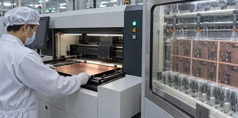
Inner-layer processing forms the conductor pattern on copper-clad cores before those layers become inaccessible. The normal sequence cleans the copper, applies photoresist, images the circuit, develops the resist, etches unwanted copper, and strips the remaining resist.
Imaging transfers the CAM-prepared pattern to the core. Laser direct imaging is common for fine registration, although the specific equipment is less relevant to the buyer than the controlled output: trace width, spacing, pad geometry, and registration targets must remain within the drawing and approved process compensation.
Etching is subtractive. Chemistry removes exposed copper while protected copper remains as the circuit. Copper thickness, feature density, line geometry, and process control affect the final conductor shape, so a nominal artwork line does not always equal the finished cross-section. The PCB etching explanation covers that mechanism in more depth; this process article keeps the focus on the release evidence.
For a single-sided or simple double-sided board, the circuit pattern may be formed on external copper rather than on buried inner cores. That shorter route removes multilayer lay-up and lamination, but it does not remove image inspection, drill registration, finish, profile, or electrical-test requirements.
The buyer rarely needs every bath log for an ordinary order. The useful evidence is an agreed acceptance standard, traceability to the correct revision, and inspection records that can identify a repeated artwork or etch problem before more value is added.
AOI, oxide treatment, and multilayer lay-up
Multilayer cores should be inspected and prepared before lay-up because a defect trapped inside the stack cannot be repaired economically later. Automated optical inspection (AOI) compares imaged copper against CAM reference data and flags opens, shorts, nicks, residual copper, or geometric anomalies for review.
Why defects must be caught before lamination
A rejected indication is not automatically a defective board. The inspection system detects differences; a trained disposition determines whether the indication violates the agreed acceptance criteria. The distinction matters because overly broad automatic rejection wastes material, while careless override allows a hidden defect into lamination. A useful outer-layer AOI evidence review uses the same principle even though the layer is inspected at a different stage.
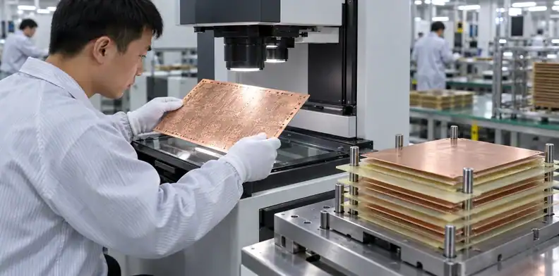
After inner-layer acceptance, the copper surface receives a bond-promoting treatment compatible with the material system. The layers are then arranged with prepreg, cores, and copper foil in the approved order. Registration targets, layer identity, foil orientation, prepreg style, and copper distribution all matter before the press closes.
| Pre-lamination gate | Evidence to retain | Why it matters later |
|---|---|---|
| Inner-layer AOI disposition | Defect map and accepted/rejected result | Buried copper cannot be visually checked after lamination |
| Layer order confirmation | Traveler or lay-up record | Reversed or swapped layers may pass a casual visual check |
| Material identity | Lot and construction record | Substitution can change thickness, Tg, CTE, or impedance |
| Bond preparation | Controlled process record | Poor adhesion may appear only after thermal stress |
| Stack symmetry review | Approved stack-up and copper balance | Imbalance can contribute to bow, twist, or movement |
The purchase specification should say whether material substitution needs approval and which stack-up characteristics are frozen. A generic note such as “equivalent FR-4 allowed” leaves too much room when impedance, thermal cycling, flammability, or customer qualification depends on the exact construction.
Lamination turns separate layers into one board
Lamination bonds the lay-up under controlled heat and pressure, while the material system cures and moves in predictable but nonzero ways. The pressing cycle must suit the resin, thickness, copper distribution, panel construction, and required final geometry.
Material movement changes finished geometry
The key buyer concern is not the press recipe itself. It is whether the approved material and stack-up produce finished dielectric spacing, total thickness, registration, and flatness that meet the released drawing. Fabricators use material behavior and process history to apply scale compensation to inner layers, but a first build or unusual construction may still need a coupon, microsection, or dimensional study.
Consider an illustrative eight-layer controller with a connector pattern controlled at two board edges. CAM shows that the released stack uses two material families and an asymmetric copper distribution. Production should pause because a generic scale factor would not prove connector-to-connector registration. A defensible action is to freeze one material set, confirm the lay-up and artwork compensation, measure the first laminated panel against internal targets, and compare the finished connector pattern with the drawing before volume release. The lesson is limited but practical: lamination approval needs construction-specific evidence when finished geometry is functionally constrained.
This scenario is not a claimed QueenEMS customer result. It shows how a fabrication hold, a measurement plan, and an approval boundary prevent a late fit dispute. If the buyer later changes material, copper balance, or finished thickness, the earlier dimensional disposition should be reopened.
A material substitution approval record is especially useful here because a laminate change can alter more than procurement availability. It may change cure behavior, resin content, coefficient of thermal expansion (CTE), loss, flammability evidence, and the compensation used to hit finished dimensions.

Drilling and hole-wall preparation
Drilling creates component holes, vias, tooling holes, and mechanical features; hole-wall preparation removes debris and resin smear so subsequent metallization can form a reliable connection. The drill program must match the released finished-hole requirements after accounting for plating and process tolerance.
Mechanical drilling is common for through holes, while laser drilling is used for microvias in qualified HDI routes. The route may also include backdrilling, controlled-depth features, countersinks, or slots. These are not interchangeable labels. Each needs geometry, side, depth, tolerance, and inspection criteria on the drawing or controlled data.
The drill does not create the finished plated-hole diameter directly. Tool size, drill wear, material stack, resin behavior, desmear, and copper deposition all contribute. That is why the buyer should specify finished hole size and tolerance rather than trying to dictate every drill tool without a functional reason.
After drilling, deburring and desmear prepare the surface and hole walls. Residual smear can interfere with connection to exposed inner-layer copper. Excessive treatment can also alter resin or glass around the hole. A microsection plan becomes useful when the construction, class, aspect ratio, thermal requirement, or customer specification makes hole quality a release characteristic.
Do not treat a clean external annular ring as proof of internal connection. The acceptance package may need cross-section evidence of hole-wall copper, inner-layer connection, resin condition, dielectric spacing, and plating quality. Those requirements should be stated before quotation so the supplier can price coupons, sample frequency, and reporting correctly.

Copper deposition and outer-layer patterning
Hole metallization creates an initial conductive path, and electroplating then builds copper on the hole walls and selected outer-layer areas. Outer-layer imaging and final etching define the external circuit while protecting the copper that must remain.
Electroless copper starts the connection
After cleaning and activation, a thin chemical copper layer makes nonconductive hole walls receptive to later electroplating. Some fabrication routes use alternative direct-metallization systems, but the control objective is the same: create continuous conductive coverage before current-driven plating begins.
Coverage quality matters more than the label on the process. Voids, poor activation, or contamination can create an intermittent connection that survives an initial continuity check and weakens under thermal cycling. The required evidence depends on the board class and purchase specification, not on a generic marketing claim.
Electroplating builds the specified conductor
Electroplating adds copper to hole walls and exposed conductor areas. Current distribution, panel design, feature density, chemistry, and process time affect thickness distribution. A single nominal value cannot describe every location on a complex panel.
The approved requirement should distinguish starting foil, plated copper, and finished copper where that distinction affects acceptance. The copper plating thickness evidence guide explains why a buyer may need coupon or microsection results instead of a statement that the line “uses 1 oz copper.”
After plating, temporary resist and etch metal are removed according to the selected process, unwanted copper is etched, and the final external pattern remains. Outer-layer AOI then checks geometry before solder mask covers much of the copper surface.

Solder mask, legend, and surface finish
These operations protect the circuit, expose intended connection areas, support assembly identification, and preserve solderable or contact surfaces. They should follow the drawing, component land pattern, assembly method, storage plan, and end-use environment.
Solder mask coats most exposed copper while leaving pads, test points, edge contacts, and other defined features open. Registration and dam width become important around fine-pitch pads. A mask opening that is easy to draw may not be stable in production, so the solder-mask opening review should happen before artwork release rather than after the first assembly defect.
Legend adds reference designators, polarity marks, revision information, and other identifiers. It must not cover pads, fiducials, exposed conductors, or controlled mechanical areas. If a marking is required for regulatory, traceability, or receiving purposes, put that requirement in the drawing instead of relying on a visual sample.
| Operation | Primary job | Buyer decision |
|---|---|---|
| Solder mask | Protect copper and define exposed features | Color, type, openings, dams, plugged/tented features |
| Legend | Support assembly and identification | Required content, sides, clearance, readability |
| HASL | Coat exposed copper with solder | Planarity and alloy compatibility for the assembly |
| ENIG or ENEPIG | Provide a planar nickel-based finish | Thickness requirement and wire-bond/contact needs |
| OSP, immersion tin, or silver | Protect copper with a thinner finish system | Storage, handling, assembly, and environment fit |
There is no universally best surface finish. Compare pad pitch, number of assembly cycles, contact function, shelf and handling conditions, and customer specification. The HASL versus ENIG decision is one common branch, but the final selection belongs to the actual product and assembly route.

Profiling, routing, and panel separation
Profiling creates the delivered outline and any routed features while preserving copper-to-edge clearance, dimensional tolerance, and a panel format that assembly can handle. CNC routing, V-scoring, punching, laser cutting, or a combined method may be used depending on material, geometry, tolerance, and volume.
The outline source must be unambiguous. If the Gerber profile, mechanical drawing, STEP model, and customer array disagree, production should stop for clarification. A closed contour also needs clear treatment for internal cutouts, plated edges, castellations, slots, bevels, and breakaway features.
Panel separation can damage a correct board when tabs, score lines, or depaneling direction put stress near brittle components or edge copper. Bare-board fabrication controls the panel geometry; assembly engineering controls how the populated panel is separated and supported. If the customer owns the array, use a formal panel drawing approval that identifies rails, fiducials, tooling holes, breakaways, coupons, and final removal conditions.
Finished dimensions should be measured against the released datum scheme. A board can fit the finished length and width while a connector edge, mounting-hole pattern, or routed pocket misses its functional relationship. State the dimension that controls fit, not only a general profile tolerance.
Packaging also starts to matter after profiling. Exposed edges, thin sections, long boards, and delicate surface finishes may need separators, rigid support, desiccant, or controlled stacking. The drawing or purchase order should name any orientation or cosmetic surface that receiving must preserve.

Electrical test and final inspection
The final gate should prove that the bare board matches the intended netlist and the agreed physical acceptance criteria before it reaches assembly. Electrical test does not replace visual, dimensional, material, or microsection evidence, and appearance does not replace net testing.
Netlist testing finds opens and shorts
Flying-probe testing suits prototypes and lower quantities because it avoids a dedicated fixture, while fixture testing can support repeated higher-volume programs. The method may differ, but the test basis should be clear: which netlist is used, what coverage is expected, and whether the purchase specification requires particular voltage, isolation, or report fields.
The PCB electrical-test requirements help define that record. A simple “E-test passed” statement is weak evidence when the netlist revision, test coverage, or retest treatment is unknown.
Final evidence must match the purchase order
Final inspection confirms workmanship and drawing-controlled features, then reconciles the shipment with quantity, revision, lot, and certificate requirements. Special characteristics may require dimensional reports, impedance results, microsections, solderability evidence, coupons, photographs, or a certificate of conformance.
| Release evidence | What it proves | What it does not prove alone |
|---|---|---|
| Electrical-test result | Intended nets have no detected opens/shorts under the test method | Material identity or dimensional fit |
| AOI record | Visible copper geometry was compared with reference data | Hole-wall integrity after plating |
| Microsection | Sampled internal construction and plating condition | Every board in the lot is identical |
| Dimensional report | Measured features meet the stated sample plan | Electrical connectivity |
| Certificate and traveler | Lot/revision/process traceability | Compliance without supporting criteria |
The release package should be proportional to risk. A simple single-sided control board and a high-reliability multilayer board do not need identical reports, but both need a defined acceptance basis and revision traceability.

Build an RFQ around the manufacturing route
A comparable PCB quotation fixes the same construction, process assumptions, test scope, and evidence across suppliers. Price differences are not meaningful when one quote assumes generic material and visual inspection while another includes a named laminate, impedance control, coupons, and documented test results.
| RFQ field | State this clearly | Why it changes the route or price |
|---|---|---|
| Revision and data format | One controlled file package | Prevents mixed-input CAM work |
| Layer count and stack-up | Copper, dielectrics, thickness, impedance | Determines imaging, lamination, drilling, and test |
| Material rule | Exact model or approved equivalency boundary | Controls sourcing and process behavior |
| Special features | HDI, filling, backdrill, edge plate, countersink, depth route | Adds qualified operations and inspection |
| Finish and mask | Type, color, controlled openings | Changes wet processing and assembly interface |
| Acceptance evidence | Class/specification, reports, coupons, sample plan | Defines what release must prove |
| Quantity and delivery | Prototype plus realistic production breaks | Changes panelization, tooling, and test economics |
IPC-6012 covers qualification and performance requirements for rigid printed boards, including single-sided, double-sided, and multilayer constructions. Referencing a standard is useful only when the revision, class or performance level, exceptions, and drawing-specific requirements are stated. Do not use a standard number as a substitute for the actual product specification.
For a route-based quotation, send QueenEMS the released Gerber or ODB++ package, fabrication drawing, netlist, stack-up, material rule, special-process notes, test evidence, and prototype/production quantities. The useful return is a quote tied to those assumptions, plus a CAM/DFM question list and any evidence that must be approved before material release.

FAQ
Are PCB manufacturing and PCB assembly the same process?
No. PCB manufacturing creates the bare board. PCB assembly applies solder paste, places components, solders them, and performs assembly inspection and functional tests after the bare board is accepted.
Does every PCB use all of these manufacturing steps?
No. A single-sided board skips inner-layer lay-up and multilayer lamination. HDI, flex, rigid-flex, filled-via, heavy-copper, and other special constructions add or alter operations.
What should a buyer approve before fabrication?
Approve the revision-controlled data, fabrication drawing, stack-up, material rule, finish, panel ownership, test requirement, and every CAM change that affects finished geometry or performance.
Which inspection step catches inner-layer defects?
Automated optical inspection checks imaged and etched inner-layer copper before lamination. It identifies differences for disposition; the acceptance standard determines whether an indication is a defect.
Is electrical testing enough to release a PCB lot?
No. It detects opens and shorts under the specified method, but it does not by itself confirm material identity, dimensional fit, hole-wall quality, finish thickness, or workmanship.
Sources
Written by the QueenEMS Engineering Team
Upload your files today · Free DFM check before production · Ship worldwide
Get your PCB prototypes in as fast as 24 hours. We handle FR4, Rogers, and hybrid boards up to 40 layers in volume production, with advanced builds subject to engineering review — free prototypes for 2–4 layer FR-4 boards, no minimum order.
Just upload your Gerber + BOM — we source every part, assemble, and inspect (AOI + X‑Ray) so you don't have to chase suppliers. Boards ship in as fast as 24 hours.