
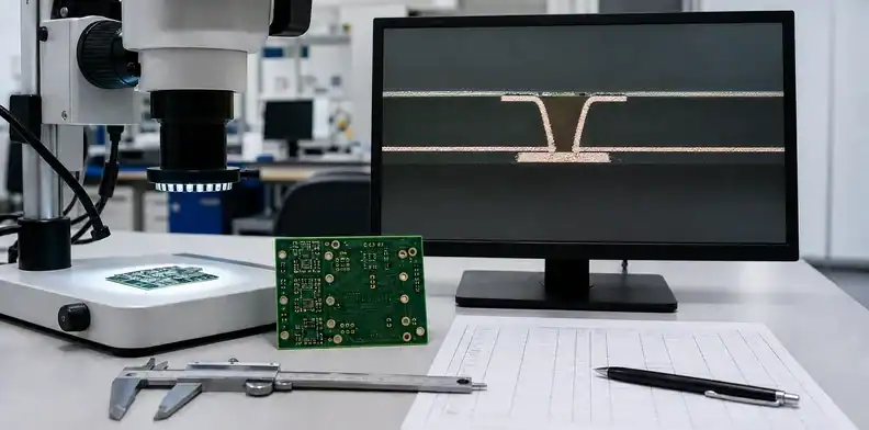
Quick Answer: PCB laser drilling acceptance should prove that every critical microvia reaches its intended capture pad without damaging the copper, trapping debris, or creating a weak interface for plating. Freeze the dielectric thickness, finished via geometry, target-pad relationship, cleaning sequence, and inspection plan before quotation. A clean electrical test alone cannot show whether the drilled and plated interface will survive assembly heat.
Laser-drilled holes are small enough that a board can look normal while the connection at the bottom of a blind via is already compromised. The buying decision is therefore not simply whether a supplier lists a minimum laser diameter. It is whether the proposed stack-up, laser process, cleaning sequence, copper deposition, and evidence plan work together for this exact construction.
This article focuses on the fabrication release decision. For broader technology selection, compare HDI PCB with a standard multilayer PCB before committing to laser-drilled build-up layers.
Table of Contents
- Define what the drilled microvia must prove
- Separate design margin from machine capability
- Account for target movement before drilling
- Inspect the via profile and capture-pad condition
- Connect drilling to cleaning and metallization
- Choose evidence that represents the risky locations
- Set sampling and disposition before production
- Control CAM and process changes
- Release a quote-ready laser drilling package
Define what the drilled microvia must prove
Acceptance rule: Release the construction only when the specified geometry and evidence demonstrate a sound target interface, not merely the presence of an electrically continuous hole.
An acceptable microvia must form a reliable electrical and mechanical interface between the plated copper and the intended target land. Hole presence and nominal diameter are only the beginning. The review also needs to address position, top and bottom diameter, taper, target exposure, debris, dielectric damage, copper damage, and the condition of the plated interface.
Write the requirement around the finished interconnect rather than around a laser machine setting. Pulse energy, focus, repetition rate, and drilling sequence are process variables owned by the fabricator. Finished geometry, target integrity, evidence, and acceptance belong in the buyer-supplier agreement.
A practical feature list includes:
- microvia start and stop layers;
- finished top and bottom diameters or an approved geometry range;
- nominal dielectric thickness being removed;
- capture-pad size and allowable positional relationship;
- whether the via is open, resin filled, or copper filled;
- whether another microvia, component pad, or controlled-impedance feature sits above it;
- required inspection and reliability evidence.
Do not reduce these fields to one note such as “laser vias per IPC.” Applicable standards establish a baseline, but they do not select the supplier’s process window or identify the locations that represent your design risk. The drawing and stack-up must still show what was designed and what must be demonstrated.
Separate design margin from machine capability
Laser placement capability cannot rescue an undersized capture pad or an unstable build-up layer. The usable margin is a tolerance stack that includes artwork registration, lamination movement, layer scaling, target-pad fabrication, laser alignment, and drilled-hole size variation. A supplier quoting only the laser’s positional accuracy is describing one contributor, not the completed relationship.
Start with the intended microvia diameter at the target and the copper available around it. Then ask how the CAM team predicts layer movement and how the chosen panel size, material system, copper distribution, and lamination cycle affect that prediction. A design that passes the HDI layout DFM checks still needs construction-specific compensation before tooling is released.
Stacked and staggered structures also change the consequence of a marginal drill. A first-level via that becomes the foundation for a second laser and copper-fill cycle needs a more controlled surface and interface than an isolated outer blind via. Use the existing stacked versus staggered microvia decision to choose the architecture; use the laser drilling acceptance plan to prove each level was formed correctly.
When margin is narrow, the appropriate response may be a larger target, a smaller finished via, a thinner dielectric, a different build-up material, a reduced panel size, or additional registration evidence. Record the approved response in the released data instead of allowing an undocumented CAM enlargement.
Account for target movement before drilling
Registration signal: Movement outside the qualified compensation window requires containment and engineering review before the laser program or capture pads are changed.
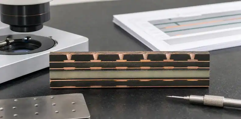
The laser drills coordinates in the panel that exists after lamination, not the ideal coordinates in the original CAD database. Resin flow, copper pattern density, glass style, panel dimensions, and press behavior can shift or distort the buried target. For that reason, target capture is partly a lamination and registration problem.
Ask the fabricator how the target layer is measured after lamination. Some constructions can use coupons, optical targets, X-ray registration, or historical scale factors. The suitable method depends on whether the buried copper is visible to the registration system and whether local distortion is significant enough that a single global scale factor is inadequate.
The buyer does not need proprietary compensation values. The buyer does need a controlled answer to four questions:
- Which layer or coupon establishes the drilling coordinate correction?
- Is compensation calculated per panel, per lot, or from a qualified construction history?
- What happens when measured movement exceeds the qualified window?
- Who approves a target-pad or artwork change proposed during CAM?
Copper balance matters because an asymmetric panel can distort differently across the sheet. When density is a concern, connect this review to the copper balance drawing approval rather than treating thieving or copper additions as invisible factory edits.
Inspect the via profile and capture-pad condition
A useful microsection shows more than a hole diameter. It should reveal the via wall profile, the opening at the dielectric surface, the condition of the target copper, residual dielectric or glass, plated coverage, and any separation at the interface. The section location and orientation must make the feature visible instead of cutting through an unrepresentative edge.
Common conditions require different dispositions:
| Observation | Why it matters | Review question |
|---|---|---|
| Residue on the target | Copper may plate over contamination without forming a durable bond | Was the post-laser cleaning process effective for this dielectric? |
| Target copper crater or penetration | Laser energy has removed or weakened the landing surface | Is the remaining copper and interface acceptable for the applicable class? |
| Severe taper or small bottom diameter | Current distribution and fill behavior can change | Does the plated geometry meet the qualified process window? |
| Glass fiber protrusion | It can obstruct cleaning and create an irregular plated interface | Is the dielectric compatible with the selected laser and cleaning sequence? |
| Positional offset | The via may lose target engagement even when it remains electrically continuous | Does the complete tolerance stack still meet the released design? |
| Copper void or interface separation | The interconnect may open during thermal exposure | What containment and expanded inspection follow? |
Define how measurements will be reported. A photo without layer names, magnification, lot identity, coupon location, and measured values is difficult to use for acceptance. The PCB microsection report requirements provide the broader report structure; the laser plan should add the microvia-specific views and fields.
Connect drilling to cleaning and metallization
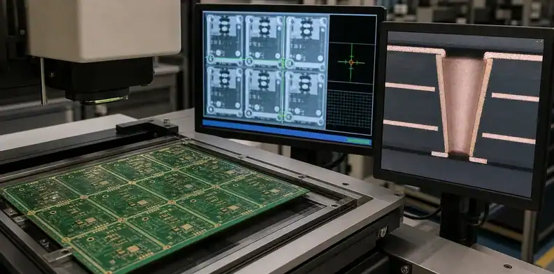
Interface check: Judge drilling, cleaning, activation, and copper deposition as one linked process because the finished microvia can fail at any boundary between them.
Laser drilling does not end when the dielectric is ablated. The target and sidewalls must be prepared for a continuous conductive deposit, followed by enough electrolytic copper or copper fill to create the specified structure. A process review that isolates drilling from cleaning and plating can miss the actual failure interface.
The cleaning method must suit the build-up dielectric and target metallization. Excessive treatment can attack resin or alter the via profile; insufficient treatment can leave residue at the bottom. The fabricator should identify the process family and demonstrate that it is qualified for the material, but the purchase drawing should avoid prescribing proprietary chemistry unless a validated customer requirement makes that necessary.
After activation and initial metallization, current must reach the bottom and walls predictably. Via aspect ratio, opening shape, panel current distribution, solution transport, and fill chemistry all influence the deposit. For structures that are filled and capped, inspect fill completeness, surface dimple, cap condition, and the interface used by the next layer.
Do not substitute outer-surface copper measurements for microvia evidence. The copper plating thickness distribution review is useful for panel-level deposition, but a laser microvia still needs evidence taken from its own geometry and process location.
Choose evidence that represents the risky locations
Evidence should represent the smallest target margin, deepest laser step, highest local via density, most difficult panel region, and any stacked structure. One easy coupon placed near the plating connection can pass while the product area with the hardest transport or greatest registration movement remains unexamined.
Build the evidence plan from the risk map:
- identify each distinct microvia construction by start layer, stop layer, dielectric and nominal geometry;
- mark which constructions are stacked, filled, capped, or under component pads;
- choose product features or coupons that represent registration and plating extremes;
- state whether evidence is required for first article, each lot, periodic qualification, or engineering change;
- name the report fields and the approval owner.
| Risk location | Representative evidence choice |
|---|---|
| Narrowest capture margin | Section or registration record through that via family |
| Deepest laser step | Profile and target-interface section for the thickest dielectric |
| Dense filled-via field | Fill and plating evidence from the transport-limited area |
| Stacked microvia level | Section that shows every plated and filled interface in sequence |
Electrical continuity is still required, but it answers a different question. A net test can detect an open circuit at the time of test. It cannot by itself prove that residue was removed, target copper remains sound, plating is bonded, or the interface will survive reflow and field cycling.
Thermal or interconnect stress testing may be appropriate when the design uses stacked microvias, multiple build-up cycles, high assembly temperature, or a reliability class that justifies additional proof. Specify the objective and specimen construction rather than requesting “thermal test data” with no link to the product.
Set sampling and disposition before production
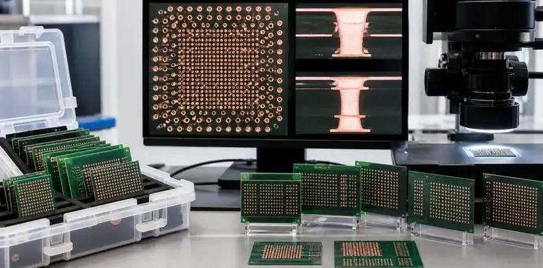
Sampling rule: The agreed plan must identify representative constructions and state the lot response before a failed section is found.
Sampling is useful only when the lot, panel position, feature family, and response to a failure are defined. “One microsection per lot” can mean very different coverage on a simple 1+N+1 board and a dense any-layer structure with several laser cycles.
State which evidence is mandatory before the lot can move forward. If a section shows marginal target capture, debris, or plating separation, the supplier response should identify affected panels, related drill programs, material batches, and process time windows. The disposition may require additional sections, non-destructive registration review, process-record review, or lot rejection. It should not default to a cropped photograph and a request for deviation.
Golden-sample approval is not a replacement for lot control. It can establish appearance and report format, but laser focus, material movement, chemistry condition, and plating performance can change. Repeat orders need a baseline that identifies what remains fixed and what evidence continues at the agreed frequency.
For prototypes, use a first-article plan that gathers learning without quietly converting provisional geometry into a production standard. Label engineering exceptions, record the revision that closes them, and require production data to reference the approved construction.
Control CAM and process changes
Microvia designs frequently trigger CAM proposals: enlarge a pad, reduce a via, add copper, change a fill method, adjust dielectric thickness, move a coupon, or alter the sequential lamination plan. Some changes are sensible, but each can affect impedance, routing clearance, assembly land geometry, reliability evidence, or repeatability.
Require a marked-up change that identifies the feature, layer, original value, proposed value, technical reason, and affected output files. The buyer’s approval should point to a named revision. When a processed dataset is returned, use processed Gerber approval to confirm that the accepted microvia edits are actually present and that unrelated geometry did not change.
Material substitution deserves the same control. A dielectric with a similar nominal thickness may ablate, clean, and plate differently. Do not carry laser settings or evidence assumptions to the substitute unless the supplier establishes an equivalent qualified window and the responsible engineer accepts it.
Once the process is frozen, repeat-order questions become easier: was the same material used, did the laser sequence change, did panelization or scale compensation change, and does current evidence match the approved baseline?
Release a quote-ready laser drilling package
Release rule: Comparable quotations require the same laser layer pairs, finished geometry, fill requirement, and evidence burden to be visible to every supplier.
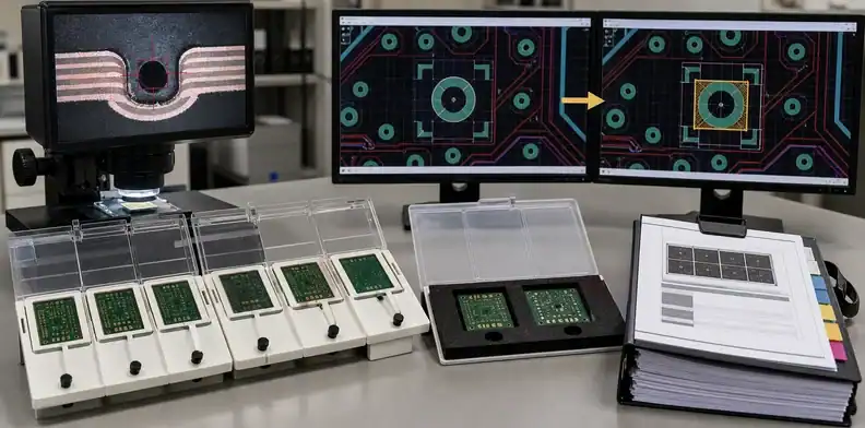
The quotation package should let suppliers price the same construction and evidence burden. Include native fabrication data or intelligent product data, fabrication drawings, stack-up, material callouts, laser drill definitions, via fill or cap requirements, panel constraints when controlled, acceptance class, and the proposed evidence plan.
| RFQ record | Minimum decision content |
|---|---|
| Laser drill table | Start layer, stop layer, nominal geometry and dielectric thickness |
| Target relationship | Released pad size, registration assumption and prohibited CAM edits |
| Finished structure | Open, filled, capped or stacked condition by via family |
| Evidence plan | Coupon location, section frequency, report fields and disposition owner |
Add a focused note that identifies:
- all laser start and stop layer pairs;
- nominal and tolerance-controlled via geometry;
- dielectric thickness associated with each laser step;
- capture-pad and via relationship that may not be altered without approval;
- fill, planarization and cap requirements;
- representative coupon or product locations;
- microsection, registration and reliability deliverables;
- first-article and repeat-lot frequency;
- named owner for CAM deviations.
Compare quotes by assumptions, not just by the stated minimum via diameter. One supplier may include per-lot sections and controlled fill evidence while another assumes visual inspection only. That difference belongs in the technical and commercial comparison before the purchase order is released.
For a quotation review, send QueenEMS the stack-up, laser drill table, pad geometry, build-up material, fill requirement, inspection plan, quantity and any proposed supplier deviations through the QueenEMS contact page. The review can then separate a genuine fabrication limit from an undocumented assumption before tooling begins.
FAQ
Can electrical test prove that a laser microvia is reliable?
No. Electrical test proves continuity and isolation at the time of test, but it does not reveal residue, marginal target capture, copper damage, weak plating adhesion, or an interface likely to open after thermal stress.
Should the drawing specify laser power and pulse settings?
Usually no. Specify the required finished geometry, target condition, material, evidence and acceptance criteria. The qualified supplier should own equipment-specific settings unless a controlled customer process has been explicitly validated.
Which microvias should be microsectioned?
Choose specimens that represent each construction and the highest-risk conditions, including narrow target margin, deep laser steps, dense areas, stacked levels and difficult panel positions. Record the chosen locations before production.
Can the supplier enlarge capture pads during CAM?
Only after the affected layers and clearances are reviewed and the change is approved in a named revision. A pad enlargement can alter routing, impedance, copper balance and component escape geometry.
Sources
- IPC, Laser Drilling a Blind Microvia
- National Library of Medicine, Ultrashort Pulsed Laser Drilling of Printed Circuit Board Materials
Written by the QueenEMS Engineering Team
Upload your files today · Free DFM check before production · Ship worldwide
Get your PCB prototypes in as fast as 24 hours. We handle FR4, Rogers, and hybrid boards up to 40 layers in volume production, with advanced builds subject to engineering review — free prototypes for 2–4 layer FR-4 boards, no minimum order.
Just upload your Gerber + BOM — we source every part, assemble, and inspect (AOI + X‑Ray) so you don't have to chase suppliers. Boards ship in as fast as 24 hours.