
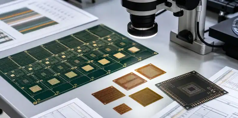
Quick Answer: BT substrate and HDI PCB are different dimensions, not two interchangeable choices. BT is a material family used in package substrates and substrate-like boards; HDI is a manufacturing and interconnect approach using microvias, sequential lamination, and fine routing.
Key takeaways
- BT is a material; HDI is a process and interconnect architecture.
- An HDI stackup can use BT, FR-4, RCC, ABF, or high-speed laminate depending on the design.
- SLP sits between advanced HDI and IC substrate work, often using lower-CTE substrate materials and finer line/space.
- The RFQ should ask for material plus process, not one word pretending to answer both.
Table of Contents
- Is BT the same as HDI?
- BT is a material; HDI is a process
- Can an HDI stackup use BT material?
- What other materials do HDI boards use?
- Where does SLP fit in?
- How PCBs evolve into IC substrates
- When should BT appear in your HDI or substrate design?
- What this means when you spec a board
Is BT the same as HDI?
No. BT and HDI answer different questions. BT answers ‘what material system is used?’ HDI answers ‘what manufacturing and interconnect structure is used?’ The two can overlap in a stackup, but they do not replace each other.
This distinction matters because many RFQs ask the wrong question. A supplier cannot quote correctly if the drawing says BT when the real need is microvia HDI, or says HDI when the real problem is substrate material.
For BT versus HDI, separate the material axis from the process axis before asking for price. HDI describes microvias, sequential lamination, and dense routing; BT describes one possible organic material system inside that build. A supplier can solve a routing problem with HDI rules, a material problem with BT, or both together, but the RFQ should not make one word carry both decisions.
The cleaner RFQ asks two separate questions: what interconnect process is required, and what material should sit inside that process. That gives CAM a route to quote and gives engineering a clear material decision.
Scope call: Do not let HDI process language replace the separate BT material decision.
This distinction also affects who should review the file. A layout engineer may focus on via stack, pad design, anti-pad clearance, and escape routing. A materials or reliability engineer may focus on CTE, moisture, Tg, and substrate stress. The supplier quote should let both reviews happen without forcing one role to guess what the other approved. The BT PCB material and sourcing guide puts this point in context with material selection, manufacturing limits, and supplier questions.
BT is a material; HDI is a process
BT substrate refers to an organic laminate material system based on bismaleimide triazine resin. HDI PCB refers to a board architecture with higher routing density, often using laser microvias, build-up layers, via-in-pad, and sequential lamination.
For process background, use the QueenEMS HDI PCB manufacturing hub. For the material side, use the BT definition page on what BT material actually is.
Supplier evidence should show both axes: HDI capability for microvias and sequential lamination, plus the proposed material family. A quote that proves only one axis still leaves the other decision open.
Evidence should be split into two lanes. The BT lane names laminate family, glass style, dielectric behavior, and material availability. The HDI lane names laser via rules, sequential lamination count, via filling, registration, and inspection method. A supplier that answers only one lane has not answered the whole RFQ.
A supplier may answer the HDI part and miss the material part, or the reverse. Push for both answers before treating the quote as complete.
Scope proof: A complete answer names both the interconnect process and the laminate family.
Can an HDI stackup use BT material?
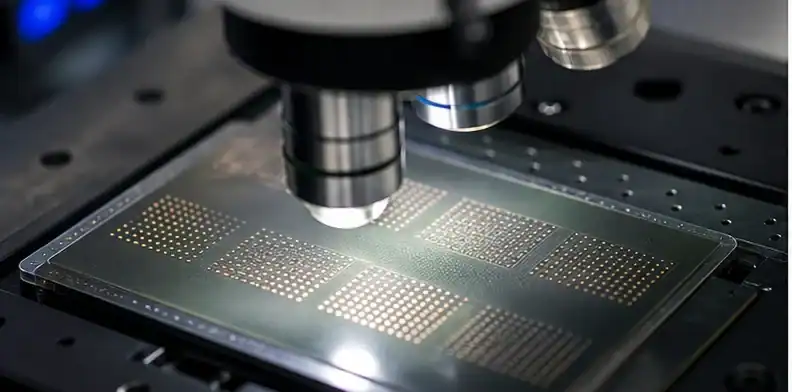
Yes. An HDI or substrate-like stackup can use BT material when the design needs its dimensional, thermal, moisture, or package behavior. It can also use FR-4 variants, RCC, ABF, or high-speed laminates when those fit better.
The quote should state both fields: material family and interconnect structure. A useful line is: ‘Please quote an HDI stackup using the proposed BT substrate material, and list any equivalent alternatives separately.’
Material values do not answer HDI capability by themselves. A board can have a good laminate and still fail the design need if microvia, registration, sequential lamination, or fine-line rules are outside the supplier’s process window.
The reverse is also true. A supplier may have strong HDI capability and still quote the wrong material branch for a package-like design. Microvias can solve fanout, but they do not define moisture absorption, expansion behavior, dielectric loss, or package reliability. When a dense board has both routing pressure and material pressure, the RFQ should show the layer build, via stack, laminate family, and test expectation together.
The data table should not merge material choice with routing process. BT values help judge laminate behavior, while HDI data comes from microvia reliability, registration, and lamination sequence. A dense board may need one axis, the other, or both; treating them separately prevents a supplier from solving the wrong problem.
Parameter review also has two lanes. Material numbers such as Tg, CTE, Dk, Df, and moisture answer the BT question; microvia reliability, line width, capture pad, and lamination sequence answer the HDI question. Keeping those lanes separate prevents a dense board from being quoted as the wrong product.
Process rule: HDI capability and BT material approval must both be checked before release.
What other materials do HDI boards use?
HDI boards do not always use BT. Many HDI boards use high-Tg FR-4, low-loss laminate, RCC, modified epoxy systems, or other material families. For high-speed designs, the QueenEMS article on matching HDI materials to signal speed is the better branch.
Material selection follows signal speed, via reliability, lamination count, board thickness, cost, and supplier capability.
This is why the material list should be tied to the design goal. Low-loss laminate may matter more than BT for a high-speed backplane. RCC may help a build-up route. High-Tg FR-4 may be enough for a dense but ordinary control board. BT becomes relevant when the dense build also needs package-like moisture, CTE, or dimensional behavior.
An HDI quote can look correct while still missing the material need. For example, microvias may solve BGA escape routing, but the laminate decision remains open if the package stress or moisture requirement points toward BT.
Write the process and material requirements as two fields: HDI route for vias and density, BT or other laminate for material behavior. Suppliers can then answer each field separately.
Decision signal: The safest response separates HDI process exceptions from BT material exceptions.
Where does SLP fit in?
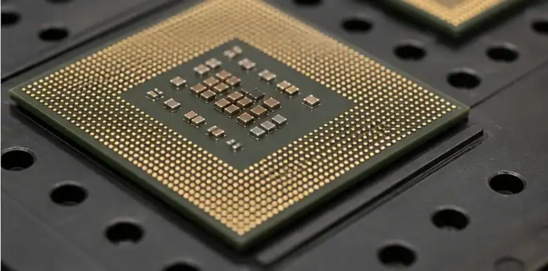
SLP, or substrate-like PCB, bridges advanced HDI and IC substrate thinking. It pushes line/space and registration tighter than ordinary HDI while staying closer to PCB manufacturing than full package-substrate production.
SLP may use BT or other lower-CTE materials when dimensional behavior matters. The buyer should ask for line/space capability, mSAP or SAP route if relevant, laser via limits, stackup tolerance, and yield evidence.
This middle category is where terminology often becomes messy. A phone module, camera module, or compact wearable board may be called HDI by one supplier and substrate-like by another. The useful engineering data is more concrete: line and space, via-in-pad, copper thickness, dielectric thickness, registration tolerance, lamination count, and whether the material must control warpage or moisture like a package substrate.
HDI cost usually comes from process complexity, while BT cost comes from material and substrate behavior. A quote can be high for either reason, so ask the supplier to separate via route from laminate route.
Separate the two price levers. HDI cost climbs with microvias, lamination cycles, via-in-pad, registration, and inspection. BT cost follows laminate choice, glass style, package behavior, and material availability. A useful supplier quote keeps those levers visible instead of blending them into one number.
Price rule: Split the HDI process cost from the BT material cost before negotiating.
How PCBs evolve into IC substrates
A practical density ladder is: multilayer PCB, traditional HDI, substrate-like PCB, then IC package substrate. Each step increases routing density, registration control, material sensitivity, and qualification burden.
That ladder helps purchasing avoid category errors. A product may need fine-pitch BGA fanout routing without needing BT. Another product may need BT material without being a full IC package substrate.
The engineering meaning is that the next step on the ladder is not always the correct step. A dense board may need one additional HDI build-up layer and a standard high-Tg laminate. Another board with less dramatic routing may still need BT because moisture or package stress is the weak point. Treat density and material behavior as separate release questions, then combine them only when the design requires both.
The approval boundary should follow the two axes. Layout or PCB engineering owns HDI geometry, material engineering owns the laminate branch, purchasing compares complete quotes, and the supplier reports exceptions on each axis.
The risk in this comparison is that the buyer may approve a process answer while the material issue remains open. Microvia capability can solve routing density, but it does not automatically solve the laminate behavior that drove the BT question.
Approval should not collapse material and process into one yes-or-no decision. Layout engineering reviews HDI geometry, material engineering reviews the laminate branch, purchasing compares complete responses, and the supplier marks whether each exception is material, via process, or layout-driven.
Approval rule: Material changes and HDI process changes need separate approval records even when they appear in one quote.
When should BT appear in your HDI or substrate design?
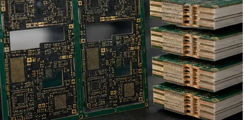
BT should appear when the material behavior is central: lower moisture absorption, package-like construction, lower expansion need, or substrate-like dimensional control. It should not appear as a default HDI buzzword.
RFQ signal: A quote-ready request names the material, line/space, via type, lamination count, copper, finish, board thickness, package pitch, and required evidence.
A weak BT-versus-HDI reply treats material and process as one decision. The safer answer splits microvia feasibility from laminate behavior, then shows whether the design needs HDI routing, BT material, or a combined dense substrate-like build.
Before moving forward, ask for one exception list for HDI process limits and another for laminate/material assumptions. Combining them hides the actual risk.
Risk check: Pause release when HDI process limits or BT material assumptions change after quote.
What this means when you spec a board
Specify the board in two layers: material requirement and manufacturing route. For example, ‘HDI with 1+N+1 build-up using approved high-Tg FR-4’ is different from ‘BT substrate with fine-line package rules.’
This prevents suppliers from quoting different products under the same label.
A dense board can need both decisions at once. The material decision controls thermal, moisture, CTE, and electrical assumptions. The HDI decision controls microvias, sequential lamination, via-in-pad, and escape routing. Ask the supplier to mark each exception as material, process, or layout. That classification helps engineering decide whether to change the stackup, reroute the BGA, adjust the material note, or move the job to a different supplier capability.
The easiest way to avoid confusion is to read the drawing in two layers. The material layer tells you what resin system, glass style, copper foil, and dielectric values are being requested. The process layer tells you whether the board uses laser microvias, sequential lamination, via-in-pad, stacked vias, thin dielectrics, and dense escape routing. BT belongs to the first layer; HDI belongs to the second.
That is why a project can be BT without being a difficult HDI board, and it can be HDI without using BT at all. A smartphone-style interconnect may use HDI techniques on other laminate families. A memory or module substrate may use BT because of package needs, even when the geometry is not described with the same vocabulary used for a mobile phone board.
SLP adds another boundary. It pushes PCB manufacturing toward substrate-like density, but it is still normally discussed as a board-level interconnect platform rather than a semiconductor package substrate. The supplier’s answer should therefore name the geometry route, the laminate family, the via process, and the inspection evidence instead of collapsing everything into one label.
For an RFQ, the drawing should make the relationship visible. A stackup table can list BT material where needed, while the fabrication notes call out HDI structures such as laser vias, sequential cycles, filled vias, or buried vias. That separation helps engineering review the design correctly: laminate substitution affects material behavior, while HDI changes drilling, plating, registration, and yield risk.
The inspection package follows the same split. Material evidence may include laminate maker, grade, Tg, dielectric data, and storage condition. HDI evidence may include microsection photos, copper plating data, via-fill confirmation, registration checks, and electrical test scope. Asking for the right evidence prevents a supplier from answering a process question with a material certificate, or answering a material question with a generic HDI capability list.
Another clue is the reason for the dense layout. A processor escape problem may be solved by HDI geometry alone, while a compact memory or module design may need BT because the package environment is driving material stability. The same via pattern can therefore lead to different supplier questions depending on the component sitting above it.
FAQ
Is BT the same as HDI?
No. BT is a material. HDI is a high-density interconnect process.
Can HDI use BT?
Yes. HDI or SLP stackups can use BT when the material requirement calls for it.
Does HDI always use BT?
No. HDI can use FR-4 variants, RCC, ABF, high-speed laminates, or other approved materials.
What is SLP?
SLP means substrate-like PCB. It sits between advanced HDI and IC substrates in density and manufacturing control.
Send QueenEMS a BT and HDI stackup clarification
For a BT-and-HDI clarification, send Gerbers, BGA pitch, line/space target, microvia plan, stackup, proposed laminate, finished thickness, finish, and inspection requirement using the QueenEMS contact page. QueenEMS can separate HDI process support from BT substrate service so the quote answers both axes.
Sources
Written by the QueenEMS Engineering Team
Upload your files today · Free DFM check before production · Ship worldwide
Get your PCB prototypes in as fast as 24 hours. We handle FR4, Rogers, and Flex up to 60 layers — free prototypes for 2–4 layer boards, no minimum order.
Just upload your Gerber + BOM — we source every part, assemble, and inspect (AOI + X‑Ray) so you don't have to chase suppliers. Boards ship in as fast as 24 hours.