Blog
PCB fabrication, PCB assembly, PCB materials, DFM, SMT, HDI, ceramic PCB, and electronics manufacturing guides from QueenEMS.
PCB Fabrication Lead Time: How Long Will Your Board Actually Take?
You submitted your Gerber files on a Tuesday, expecting bare boards on your desk by Friday, only to receive an automated notification…
Guide to PCB Fabrication Cost: How to Save on Your Quote
Table of Contents You just designed a new board, and now you are wondering about the actual PCB fabrication cost before sending…
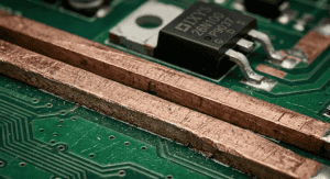
Heavy Copper PCB Design: Copper Weight, Trace Width and Layout Rules
Heavy copper PCB design means laying out boards with thick copper, usually 3 oz/ft² (about 105 µm) or more per layer, to…
What PCBA Approved Alternates Need Before Release
Decide how PCBA approved alternates should be listed, reviewed, sourced, and locked before production release….
7 Reasons for PCB Prototype Failure (And How to Prevent Each One)
You open the shipping box, plug in your freshly assembled board, and… nothing happens. Or worse, you see the magic smoke. A…

DFM PCB Design Checklist: Fabrication, Assembly and Release
A practical DFM PCB design checklist for fabrication, assembly and controlled manufacturing release….

How China vs USA PCB Assembly Choices Work
China vs USA PCB assembly compared by build stage, landed cost, sourcing control, quality evidence, testing scope, and release-package maturity….
What PCB Assembly Quote Files Do You Actually Need?
Table of Contents You just finished routing your board and sent the design off to three different manufacturers. One replies with a…
PCB Assembly Cost: What a Quote Includes and How to Compare It
Quick Answer: PCB assembly cost is not one reliable dollar-per-board number. A useful quote separates bare boards, components, one-time setup and stencil,…

How to Create a Flawless BOM for PCB Assembly (Free Template)
You just finished your board design, generated the files, and hit send. But if your BOM for PCB assembly is messy, you…
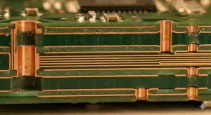
Prepreg PCB Guide: 10 Secrets To Flawless Board Stackups
The material known as prepreg is a dielectric insulator made of woven fiberglass impregnated with partially cured epoxy resin. Are unpredictable impedance…
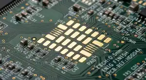
ENIG Surface Finish: IPC-4552B, Black Pad and How to Specify It
ENIG (electroless nickel immersion gold) is a PCB surface finish made of a layer of nickel plated onto the copper pads, then…