
Blog
PCB fabrication, PCB assembly, PCB materials, DFM, SMT, HDI, ceramic PCB, and electronics manufacturing guides from QueenEMS.
HASL vs ENIG PCB Finish: Flatness, Black Pad and When to Use Each
HASL coats the copper pads with solder by dipping the board and leveling it with hot air; ENIG plates a layer of…

HDI PCB vs Standard PCB: Cost, Routing and Reliability
A practical comparison of HDI and standard PCBs based on routing, fabrication, reliability and total delivered cost….

Rigid-Flex vs Flexible PCB Cost: What Drives It and When Each Pays Off
A flexible PCB is a circuit built entirely on flexible film, usually polyimide; a rigid-flex PCB laminates rigid board sections and flexible…

How to Get PCB Stack-Up Design Right Before Fabrication
PCB Stack-Up Design needs more than a layer drawing. Check layer order, reference planes, dielectric thickness, impedance targets, vias, materials, and fab notes….
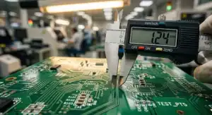
PCB Fabrication Tolerances: Which to Specify and Which to Pay For
PCB fabrication tolerances are the allowed variation between the board you designed and the board you receive: hole sizes and positions, trace…
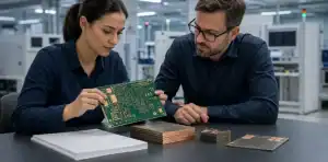
How to Choose a PCB Manufacturer for Your Board
Review draft for post 1865: choose a PCB manufacturer by checking board capability, evidence, quote scope, prototype approval, and production controls….

PCB Copper Weight Cost: When Do You Actually Need 2oz?
You are laying out a power delivery network for a new motor controller, staring at your CAD screen, wondering if you should…
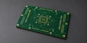
How to Check PCB Fabrication Defects Before Assembly
Check PCB fabrication defects before assembly with symptom-specific evidence, drawing requirements and a documented decision for suspect bare-board lots….

PCB Trace Width & Spacing Guide: Rules, Charts & Calculator
You just finished routing a dense microcontroller board with 4mil traces, feeling proud of the compact layout. Then, your manufacturer kicks the…

PCB Warping Causes: Why Your Boards Bend & How to Stop It
You unpack a fresh batch of circuit boards, set one on your workbench, and notice it wobbles like a bad diner table….

2 Layer vs 4 Layer PCB: Differences, Cost, Lead Time and How to Choose
A 2-layer PCB has copper on the top and bottom only, so signals, power and ground share the same two layers. A…

How to Make Your PCB Prototype Order Fab-Ready
Quick answer: Before you order PCB prototype boards, define what the build must prove and release one coherent file set. A bare-board…