
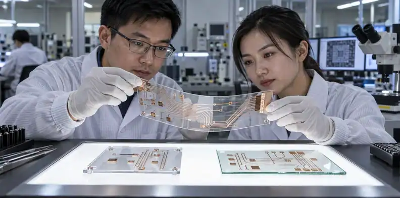
Quick Answer: A transparent PCB can mean a clear flexible circuit, a clear rigid substrate, a glass or transparent ceramic circuit, or a circuit that also uses transparent conductors. These architectures do not offer the same optical clarity, soldering window, flexibility, circuit density, or cost. Define the optical path, acceptable visibility of copper and components, electrical load, bend condition, assembly process, environment, and prototype acceptance sample before requesting a production quote.
Transparency is a system requirement, not a board color. A clear base film may still carry opaque copper traces, plated pads, solder, components, stiffeners, and connectors. A circuit that looks transparent in a product photograph may block the exact region needed for a camera, display, light guide, sensor, or illuminated surface.
The market is also changing quickly. Recent search results mix PET flex circuits, clear rigid laminates, glass, ceramic, indium tin oxide (ITO), and metal-mesh electrodes under one keyword. A reliable specification separates those technologies, then chooses the simplest architecture that meets both the optical and electrical job.
Table of Contents
- Define what must be transparent
- Transparent flex, rigid, glass, or ceramic
- Clear substrate does not mean clear conductors
- Optical targets compete with circuit density
- Thermal limits depend on the material system
- Bend behavior separates PET and polyimide options
- Surface finish and assembly remain visible
- Prototype the optical and electrical system
- Common transparent PCB requests that fail review
- Prepare a transparent PCB RFQ
Define what must be transparent
Start by marking the optical keep-clear region, viewing direction, wavelength range, lighting condition, and acceptable visual obstruction. “Transparent board” does not tell the supplier whether the product needs a clear window, an attractive visible circuit, low haze over a display, or a nearly invisible conductor.
Optical path and visual appearance are different
A decorative product may welcome visible copper as part of the design. A camera, optical sensor, display, or light guide may reject the same trace even when the surrounding film looks clear. State whether the requirement is functional transmission, cosmetic appearance, or both.
| Optical input | Question to answer | Evidence at prototype |
|---|---|---|
| Clear area | Which exact region must pass light? | Dimensioned overlay or optical keep-out drawing |
| Viewing direction | Normal, angled, one-sided, or both sides? | Product-level visual inspection setup |
| Wavelength | Visible light or another optical band? | Measurement method and range |
| Haze and color | What change is acceptable? | Approved reference sample |
| Visible metal | Are copper, pads, finish, and components allowed? | Render plus assembled prototype |
Add the enclosure, lens, adhesive, protective film, coating, and display stack to the optical review. These layers can change reflection, haze, color, or bubbles even if the bare circuit meets its own requirement.
QueenEMS can review transparent PCB projects, but the capability decision must be tied to a specific construction and acceptance target. Without a layer structure and optical requirement, a yes/no capability answer would hide the variables that determine whether the product works.

Transparent flex, rigid, glass, or ceramic
The substrate architecture determines the manufacturing route, mechanical behavior, conductor options, assembly method, and realistic optical result. Do not treat the four common paths as interchangeable materials.
The substrate choice changes the manufacturing route
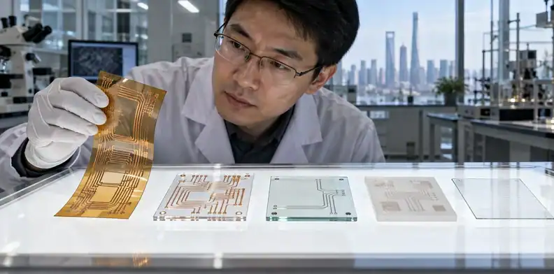
Transparent flexible circuits usually use a clear polymer film and patterned conductors. A transparent rigid PCB uses a rigid clear laminate or another qualified transparent base. Glass circuits can support optical products but require processes suited to a brittle inorganic substrate. Transparent ceramic circuits use a translucent or transparent ceramic system where thermal, dielectric, or optical behavior justifies the specialized route.
Clear flexible circuits are thin and conformable, but bend life, heat, visible copper, and dimensional stability must be resolved. A clear rigid board preserves a familiar form while introducing material availability, haze, multilayer blockage, and process limits. Glass offers optical and dimensional potential but adds brittleness, edge handling, interconnect, and assembly questions. Transparent ceramic belongs to a specialized thermal, dielectric, and metallization route. A transparent-electrode device can reduce visible conductor area, yet sheet resistance, current, contact, patterning, and environmental durability become new constraints.
The flexible PCB manufacturing route is the natural starting point when the product must bend or wrap. If heat removal is the main problem rather than optical transmission, compare the requirement with an aluminum PCB for LED systems instead of forcing a transparent material into a thermal role it cannot support.
Transparent ceramic belongs to another decision family. The ceramic PCB material comparison discusses thermal-material trade-offs, but a transparent ceramic project still needs a separate optical and metallization review.
Clear substrate does not mean clear conductors
Conventional copper traces, plated pads, surface finish, solder, and components remain visible even when the substrate is clear. The optical layout must therefore treat metal coverage as a design variable.
Copper traces remain visible
Narrower traces block less area, but electrical current, voltage drop, heating, manufacturability, and reliability set a lower boundary. Moving traces outside the optical window may be safer than reducing them until they lose margin. Mesh or sparse routing can change visual appearance, yet the current path and connector transition still require solid engineering.
Ground planes and broad power copper are especially important. A multilayer transparent board can become visually opaque when internal planes overlap, even if every dielectric is clear. If the product needs a ground reference or shielding, decide whether optical transparency or electrical performance has priority in each region.
Transparent electrodes are a different technology
ITO, metal mesh, nanowire, conductive polymer, or other transparent-electrode approaches trade optical transmission against sheet resistance, current density, pattern resolution, contact resistance, bending, adhesion, oxidation, and process compatibility. They are not drop-in replacements for standard PCB copper.
Published research on copper mesh transparent electrodes shows why geometry matters: the conductive network and open area jointly determine electrical and optical behavior, while bending and environmental stability require their own tests. A research result does not prove a production capability or approve the contact system for your product.
| Conductor question | Conventional copper | Transparent-electrode path |
|---|---|---|
| Optical obstruction | Clearly visible and often dominant | Reduced through sparse or optically transmissive structure |
| Current capability | Familiar PCB design methods | Must be verified from sheet resistance and geometry |
| Solder/termination | Established finishes and land patterns | Often needs a specialized contact or transition |
| Environmental risk | Finish, corrosion, adhesion, flex fatigue | Adds film/mesh adhesion and contact stability |
| Supplier route | Conventional PCB/flex fabrication variant | May require display, printed-electronics, or research process |
Optical targets compete with circuit density
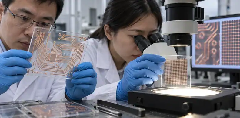
Every trace, pad, component, via, stiffener, label, and plane consumes optical area or creates a visible feature. The layout should reserve the optical window before routing rather than trying to clear it after the circuit is complete.
| Design choice | Optical effect | Electrical or manufacturing trade-off |
|---|---|---|
| Wider clear keep-out | More unobstructed area | Less routing and component space |
| Narrower copper traces | Less visible metal | Higher resistance and tighter process margin |
| More layers | More routing freedom | Greater overlap and reduced apparent clarity |
| Smaller components | Lower visual blockage | Assembly, sourcing, inspection, and rework complexity |
| Hidden edge connector | Cleaner center window | Mechanical and cable constraints at the perimeter |
Place LEDs, sensors, cameras, displays, and light guides in the mechanical model with their fields of view and emission paths. Copper behind an LED may reflect usefully in one design and create glare in another. A transparent circuit must be evaluated as part of the product’s optical stack.
Avoid cosmetic silkscreen or broad legend fields in the clear region. If identification is required, move it to a border or define a minimal mark. Solder mask or protective film may look clear in one thickness and hazy over copper relief, adhesive flow, or surface texture.
The PCB DFM review before purchase order should include an optical overlay: clear zone, allowed conductor zone, component shadows, fiducials, tooling, stiffeners, connectors, and any appearance-critical face. That prevents production additions from occupying a space the optical team assumed was empty.
Thermal limits depend on the material system
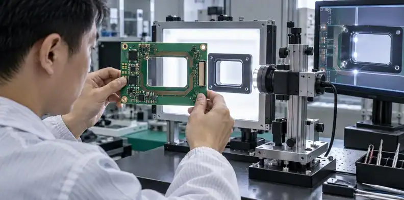
Transparent polymer, rigid laminate, glass, ceramic, conductor, adhesive, finish, and component system can each set a different thermal boundary. Do not use one vendor’s peak number as the service rating for a different construction.
Assembly temperature is not service temperature
A short soldering exposure, repeated reflow cycles, continuous powered operation, outdoor solar load, and storage at temperature stress materials differently. State all of them. The supplier should identify which stage controls the construction and whether assembly uses standard reflow, low-temperature solder, conductive adhesive, local soldering, or another route.
Clear PET-based flex can offer strong optical appearance and cost advantages for suitable products, but its processing and service behavior must be checked against the assembly profile. Clear or modified polyimide may provide a different balance of heat and flexibility. Glass and ceramic tolerate other thermal conditions but introduce brittle mechanics and specialized metallization.
Heat from LEDs, drivers, resistors, or charging circuits can create local yellowing, distortion, adhesive movement, conductor resistance change, or solder-joint stress even when ambient temperature looks acceptable. Build a heat path through copper, a separate spreader, chassis contact, airflow, or product architecture rather than assuming a transparent substrate also acts as a heatsink.
For concentrated light or power, the ceramic PCB for high-power LED decision provides a useful alternative architecture. The transparent requirement should survive only when light passage or visual design creates real product value.
Bend behavior separates PET and polyimide options
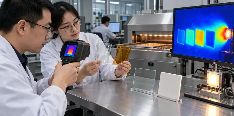
A transparent flexible circuit must be selected for its installed bend, repeated motion, conductor geometry, adhesive system, and terminations, not merely because the film can bend by hand. PET and transparent polyimide constructions can differ in heat, dimensional, optical, and mechanical behavior.
For a static fold, define radius, angle, direction, and installation sequence, then inspect a fitted sample after forming. Dynamic motion adds flex length, axis, speed, and cycle count and should be tested with continuity monitoring. A twisting path needs rotation, unsupported length, and cable restraint in a product fixture. Stiffener transitions require material, position, setback, and thickness records. Connector terminations need mating geometry, insertion, retention, and cycling verification.
Copper grain direction, trace direction, pad transitions, coverlay openings, and stiffener edges influence flex fatigue. Routing traces across a bend, placing vias in a dynamic region, or allowing a stiff bond edge to enter motion can fail even when the base film remains intact.
The flex PCB stiffener requirements apply when a transparent tail mates with a ZIF connector or supports a local component. A visible stiffener may be acceptable at the edge but unacceptable in the optical field, so the mechanical and cosmetic drawings must agree.
A flexible transparent construction can use IPC-6013 as its base performance specification. State the applicable revision and product requirement, then add the project-specific bend, optical, environmental, and appearance acceptance that the standard reference does not select for you.

Surface finish and assembly remain visible
Pads, finish, solder joints, components, flux residue, underfill, PSA, and coating can dominate the appearance of an assembled transparent PCB. Approve the assembled visual result, not only an unpopulated material sample.
Appearance samples need production controls
A photograph can hide haze, reflection, color shift, copper roughness, adhesive bubbles, scratches, and edge marks. Define an inspection setup: background, illumination, viewing angle, distance, clean area, acceptable sample, and functional optical measurement where required.
Surface finish should follow soldering and contact needs. HASL, ENIG, ENEPIG, OSP, immersion tin, immersion silver, hard gold, or a specialized contact may look different and change pad planarity or color. The HASL versus ENIG comparison can inform one branch, but transparent appearance adds its own sample approval.
Copper density, finish type, and an appearance sample should control the visible metal, while receiving checks color, coverage, oxidation, and scratches. Solder mask or cover film needs a named material, thickness, openings, and clear-zone boundary, followed by checks for haze, bubbles, registration, and contamination. Component packages, orientation, and solder route set the assembled appearance. Stiffeners and PSA need controlled outlines, liners, and edges. Keep legend content minimal and confined to an approved zone.
Protective films and separators may be needed during shipment. Clear surfaces show scratches, fibers, fingerprints, dust, and rub marks readily. Packaging instructions should define which liner remains, which face is appearance-critical, and how receiving handles the part before assembly.
Prototype the optical and electrical system
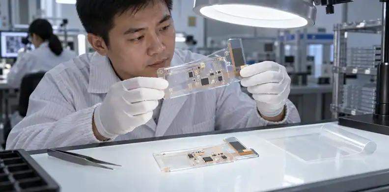
A transparent PCB prototype should prove optics, circuit performance, assembly, mechanics, environment, and appearance in the real product stack. A bare film held against a window is not enough.
Use a witness panel and acceptance sample
Include optical coupons or witness regions when they help compare material, conductor density, cover film, or process variation. Preserve one approved assembled sample under controlled storage and record the lighting and measurement method used for acceptance.
An illustrative wearable display project may request a transparent flex over an illuminated window. The first layout routes a broad ground conductor through the center, meets electrical continuity, and looks acceptable on a white desk. Inside the product, angled illumination turns the conductor into a bright reflection that obscures the display. The proper action is to map the real optical path, move or reshape copper outside the critical field, verify return-current behavior, and retest the assembled optical stack at operating temperature and bend condition.
This is an illustrative scenario rather than a claimed QueenEMS case. The expected improvement remains conditional until the revised prototype passes both optical and electrical acceptance. Moving the conductor without checking return current could solve glare and create an EMI problem.
The prototype plan should include electrical load, voltage drop, temperature, continuity during bending, connector cycling, optical transmission or haze method, cosmetic inspection, assembly yield observations, and environmental exposures relevant to use. Tie every result to the material lot, stack-up, artwork revision, finish, assembly route, and inspection setup.
The PCB prototype quote review can help keep sample and production assumptions visible. Transparent material availability, custom tooling, appearance sampling, and specialized assembly may make a prototype quote structurally different from a standard rigid PCB quote.

Common transparent PCB requests that fail review
Most early holds come from an undefined architecture, an impossible optical/electrical trade-off, or a missing assembly and acceptance plan. Resolving the request in engineering terms is faster than asking several suppliers for an unsupported yes/no answer.
| Request that causes a hold | Missing decision | Better RFQ statement |
|---|---|---|
| “Make the whole PCB invisible” | Allowed metal, component, connector, and shadow areas | Dimension the functional clear zone and visible features |
| “Use transparent FR-4” | Rigid material identity and required optical result | State architecture as proposed and allow material review |
| “Use the same stack-up as our normal board” | Clear-material availability and process compatibility | Supply electrical requirements and approve a new stack-up |
| “Support reflow and outdoor use” | Thermal cycles, service profile, UV/moisture condition | Provide assembly and mission profiles separately |
| “Four layers with high transparency” | Plane coverage and optical path | Mark clear regions and required reference/power structure |
Another common failure is using a competitor’s published layer count or transmittance as a universal industry capability. Those numbers belong to a named material, thickness, geometry, process, measurement method, and date. QueenEMS should confirm the current project instead of repeating them.
Material substitution also needs control. A clear film from another supplier can change haze, color, surface treatment, adhesion, dimensional behavior, and assembly compatibility. Use the PCB material substitution approval process and include the optical properties that ordinary PCB substitution records may omit.
Stop production when the approved appearance sample, material, optical zone, conductor pattern, finish, or assembly route changes. Cosmetic transparency is not a minor preference when it is part of the product function or customer acceptance.

Prepare a transparent PCB RFQ
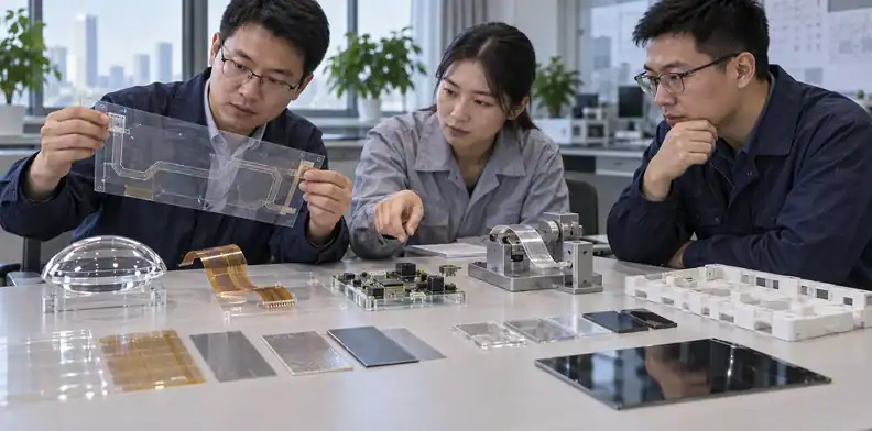
A quote-ready package defines the architecture or permits a documented proposal, then supplies the optical, electrical, mechanical, thermal, assembly, environmental, and appearance requirements needed to evaluate it. Keep open requirements visible instead of filling them with copied vendor specifications.
| RFQ field | What to provide | What QueenEMS engineering should return |
|---|---|---|
| Product optical stack | Enclosure, lens/display/light path, clear-zone drawing | Feasible board architecture and open optical risks |
| Circuit requirements | Schematic intent, current, voltage, interfaces, grounding | Conductor and layer proposal with limitations |
| Mechanical use | Outline, thickness, static/dynamic bend, connector, support | Material/construction and prototype conditions |
| Thermal and environment | Assembly profile, service/storage, UV, humidity, chemicals | Compatibility gaps and validation plan |
| Appearance | Allowed copper/components, haze/color method, sample setup | Inspection method and approval sample plan |
| Commercial scope | Prototype quantity, production forecast, assembly inclusion | Quote assumptions, tooling, lead-time dependencies |
Send Gerber or ODB++, a fabrication drawing, stack-up proposal if one exists, 3D product context, optical overlay, BOM/assembly plan, and acceptance tests under one revision. State which items are fixed and which may be proposed. A transparent-conductor request should explicitly identify whether standard copper is unacceptable and what sheet resistance/current/contact result is required.
For project review, send QueenEMS the clear-zone drawing, optical stack, accepted visibility of copper and components, circuit load, bend profile, assembly temperature history, environmental exposure, prototype test plan, and volume estimate. The response can identify a feasible transparent PCB route, required material or process confirmation, prototype gates, and quotation assumptions without inventing a universal capability table.
FAQ
Is a transparent PCB completely invisible?
No. The substrate can be clear while copper traces, pads, finish, solder, components, connectors, and stiffeners remain visible.
Are transparent PCBs always flexible?
No. Transparent circuits can use flexible polymer films, rigid clear laminates, glass, ceramic, or specialized transparent-electrode structures.
Can a transparent flexible PCB use ordinary copper?
Yes, many clear flex constructions use visible copper conductors on a transparent substrate. The layout must balance optical open area with current, resistance, heat, and manufacturing limits.
Can transparent PCB material pass a normal SMT reflow?
Only when the exact substrate, adhesive, finish, component, and assembly process are qualified for the proposed thermal history. Do not transfer a vendor’s number to another construction.
What should I send for a transparent PCB quote?
Send the optical clear-zone and measurement requirement, circuit data, layer/conductor intent, mechanical and bend conditions, assembly profile, environment, appearance sample plan, prototype quantity, and production forecast.
Sources
- IPC-6013: Qualification and Performance Specification for Flexible Printed Boards
- Cu Mesh for Flexible Transparent Conductive Electrodes
Written by the QueenEMS Engineering Team
Upload your files today · Free DFM check before production · Ship worldwide
Get your PCB prototypes in as fast as 24 hours. We handle FR4, Rogers, and hybrid boards up to 40 layers in volume production, with advanced builds subject to engineering review — free prototypes for 2–4 layer FR-4 boards, no minimum order.
Just upload your Gerber + BOM — we source every part, assemble, and inspect (AOI + X‑Ray) so you don't have to chase suppliers. Boards ship in as fast as 24 hours.