
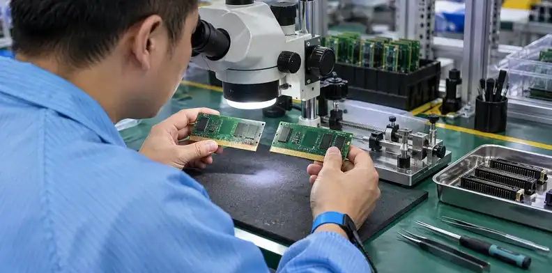
Quick Answer: PCB gold finger repair is reasonable when the problem is removable contamination, shallow wear on an intact contact, or a locally damaged finger that a qualified technician can rebuild and verify. Replace or rebuild the board when heat, arcing, delamination, broken internal connections, widespread wear, or an uncorrected mating-connector fault makes the repair unreliable. Record the condition before cleaning, match the method to the damage, and define the acceptance test before work begins.
A card that works after reseating and fails again a week later does not yet have a repair diagnosis. The fault may be skin oil, dried process residue, a worn socket, exposed nickel, a lifted contact, a cracked edge, or electrical damage below the visible surface. Each condition needs a different response.
This article gives engineering, quality, maintenance, and purchasing teams a controlled way to choose among cleaning, professional repair, and board replacement. It focuses on the disposition after damage. Design rules, original plating acceptance, and finish selection stay with the linked QueenEMS resources that own those subjects.
Table of Contents
- What Damage Can PCB Gold Finger Repair Address?
- What Evidence Should You Capture Before Cleaning?
- When Is Cleaning Enough?
- Which Damage Needs Professional Replating?
- When Can a Missing Edge Contact Be Rebuilt?
- When Is Board Replacement the Safer Choice?
- How Should Repair vs Replacement Be Approved?
- How Do You Verify a Repaired Gold Finger?
- How Can You Prevent Repeat Damage?
- What Should You Send for a Replacement PCB Quote? – FAQ
What Damage Can PCB Gold Finger Repair Address?
PCB gold finger repair can address a limited set of contact defects. Removable films may need only cleaning. Shallow scratches or worn plating may qualify for controlled selective plating when the base contact remains sound. A missing or lifted finger may qualify for a bonded replacement contact when the connecting circuit and laminate can support it. Heat damage, deep substrate loss, or repeated failure often calls for a replacement board.
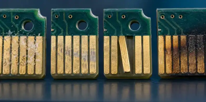
Start with the physical layer that failed. A dark mark on top of intact gold is different from nickel or copper showing through the wear track. A clean break at one contact is different from a charred edge that may contain carbonized laminate and damaged internal copper. A shiny solder smear is not ordinary dirt. Treating all four as a cleaning problem can erase useful evidence or enlarge the defect.
PCB gold finger corrosion usually describes attack on nickel or copper exposed by a pore, scratch, or worn gold layer, not corrosion of intact gold. When PCB gold finger damage includes that base-metal change, cleaning may remove residue but cannot restore the missing barrier and wear surface.
The classification below is a triage tool, not a release specification. Drawings, product class, contract controls, and the responsible engineering authority still decide whether any repair is acceptable.
| Observed condition | Likely first action | Repair path to evaluate | Hold or replace when |
|---|---|---|---|
| Fingerprint, dust, light removable film | Document, then use an approved cleaning process | Cleaning and re-test | Residue returns, plating is discontinuous, or the fault remains |
| Shallow scratch or worn gold with flat, intact metal | Inspect under magnification | Professional selective replating | Deep nick, pinhole, missing metal, or damaged substrate is present |
| Local solder contamination | Preserve evidence and assess heat history | Controlled stripping and replating | Heat damage, lifted copper, or geometry loss is present |
| One lifted or missing contact | Map the connected circuit and bonding surface | Film-adhesive or approved epoxy contact replacement | The base material is burned, uneven, delaminated, or too weak to bond |
| Multiple burned contacts or damaged laminate edge | Stop use and inspect the mating connector | Replacement board or controlled rebuild | Repair cannot restore geometry, insulation, and repeatable mating |
For construction and finish background, use the existing PCB gold fingers design and reliability article rather than expanding this repair decision into a second general page.
What Evidence Should You Capture Before Cleaning?
Capture the failure state before a swab, eraser, abrasive, or solvent touches the connector. Photograph the board and mating slot, record the symptom and operating conditions, mark the affected contacts, note the board revision and serial or lot identity, and preserve the electrical test method. Cleaning may remove residue, wear debris, or an arc track that points to the root cause.
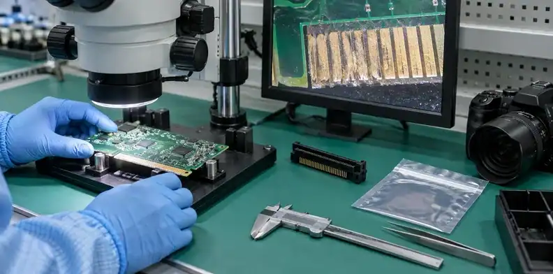
Take one full-edge image for orientation and close images under consistent light. Include a scale or microscope calibration when dimensions matter. Photograph the slot or backplane contacts as well. If damage appears at one end of the card edge, a misaligned guide, damaged spring contact, or uneven insertion force may be more relevant than the visible gold color.
Electrical readings need context. A handheld continuity beep can find an open circuit, but it cannot prove a low-resistance mating interface. For low values, a four-wire method can remove much of the test-lead error. Compare the result with the controlled drawing, the connector or system requirement, an approved golden unit, or the same method used on known-good contacts. Do not substitute an internet milliohm number for the product’s acceptance rule.
| Evidence to record | Minimum useful detail | Why it changes the decision |
|---|---|---|
| Board identity | Part number, revision, serial/lot, assembly state | Prevents mixing limits or histories from different revisions |
| Failure symptom | Slot, channel, temperature, load, movement, intermittent pattern | Separates contact trouble from another circuit failure |
| Visual condition | Full edge plus close images before cleaning | Preserves residue, wear track, exposed metal, and heat evidence |
| Mating hardware | Connector part/slot, bent or contaminated contacts, alignment | Shows whether the socket will damage a repaired board again |
| Electrical baseline | Instrument, fixture, lead method, test points, known-good comparison | Makes the before/after result repeatable |
| Service history | Insertion count if tracked, prior cleaning/repair, repeat rate | Exposes recurrence and cumulative damage |
If the symptom involves more than the connector, use a structured PCBA failure analysis report to keep observations, suspected cause, verification, and corrective action separate.
When Is Cleaning Enough?
Cleaning is enough only when the contaminant can be removed without changing the contact geometry or plating, and the board then passes the same test that exposed the fault. A cleaner-looking surface is not proof of a serviceable connector. Inspect it again, test it using the recorded method, and mate it only in a connector that has also been checked.
Use a Controlled Cleaning Sequence
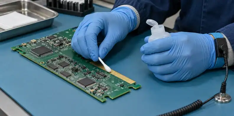
De-energize and remove the board using the product’s ESD and handling controls. Keep bare fingers away from the contact face. Use a cleaner approved for the assembly materials and the contaminant, with a low-lint swab or wipe that does not shed into the slot. High-purity isopropyl alcohol is commonly selected for compatible electronics because suitable grades dry quickly and leave little residue, but it is flammable and absorbs moisture after opening. The assembly’s material compatibility, ventilation, PPE, and drying requirements still control the process.
Apply the minimum mechanical force needed to lift the film. A pencil eraser, coarse abrasive, metal polish, or uncontrolled fiberglass brush may make the contact look brighter by removing part of the plated surface. That changes the part you are trying to preserve. Teams asking how to clean PCB gold fingers should define the chemical, applicator, stroke direction, drying time, and inspection step before touching production hardware.
Where process residue or ionic contamination is suspected, connect the cleaning action to the site’s documented PCB cleanliness testing requirements instead of assuming that visual cleanliness proves the residue is gone.
Stop if the Surface Changes After Cleaning
After cleaning and drying, inspect under the same light and magnification used for the baseline. Stop if the wiped area reveals a different metal color, a groove that catches light, a raised edge, a loose contact, blistering, a crack, or a darkened substrate. Those findings move the case from contamination removal to metal or base-material repair.
Repeat the electrical and functional check without changing several variables at once. If cleaning the board and replacing the socket happen together, the team cannot tell which action fixed the fault. A board that passes one insertion but fails after slight movement also needs more work. Record the cleaned condition, test result, connector used, and release decision so the next failure does not restart the diagnosis from memory.
Which Damage Needs Professional Replating?
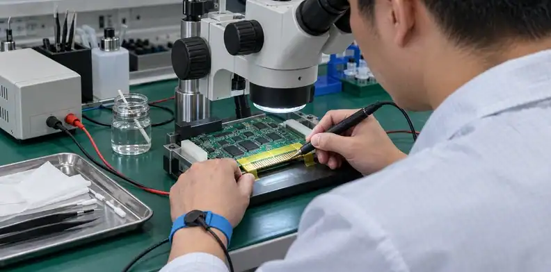
Professional gold finger replating fits surface damage when the copper contact remains present, flat, electrically connected, and free of deep defects. The process may be appropriate for shallow scratches, plating wear, a finish below the approved requirement, or solder contamination that can be stripped without damaging the contact. It does not replace missing metal or rebuild a damaged laminate edge.
Selective plating is a controlled electrochemical repair. The technician masks nearby areas, creates a reliable electrical bus to the contacts, prepares the surface, deposits the required barrier and gold layers, rinses between steps, and measures the result. A plating kit by itself does not define the alloy, thickness, hardness, adhesion, coverage, or acceptance evidence needed by the product.
Place the job on hold when the contact has deep scratches, nicks, pinholes, loose copper, exposed glass fibers, char, or uncertain base-metal condition. Large defects can trap chemicals or leave a nonuniform surface even if the new gold looks continuous. Solder on the mating face is also not a permanent wear surface. It changes hardness and geometry and can transfer material into the connector.
Before release, tie the method to the original drawing or an approved deviation. The existing PCB gold finger plating acceptance page covers the buyer evidence that belongs in the drawing and shipment review. When the disposition depends on measured nickel or gold, use the surface-finish thickness evidence article to define what the report must identify. Do not accept “replated” as a complete inspection record.
When Can a Missing Edge Contact Be Rebuilt?
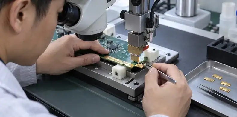
A missing edge contact can sometimes be rebuilt when the connecting conductor is identifiable, the bonding area is flat and stable, the board edge can be restored to the required profile, and the product allows a repaired contact. This is advanced work. The replacement must align with adjacent contacts, survive insertion force, connect electrically without a vulnerable joint in the wear area, and remain compatible with the mating connector.
Film-Adhesive Contact Replacement
The film-adhesive method uses a prefabricated nickel-and-gold-plated contact with a dry adhesive layer on its back. The technician removes the damaged contact, cleans and levels the bonding area, exposes a controlled length of the connected circuit, trims and aligns the replacement, bonds it with specified heat and pressure, completes the electrical connection, and files the overhang to match the board edge. Visual alignment, contact width and spacing, bond condition, and electrical continuity all belong in the evaluation.
The flatness requirement deserves attention. A plated foil cannot hide a gouged laminate edge. If glass fibers are exposed, the bonding surface is depressed, or the edge has lost material, base-material repair may be needed before a contact can be attached. The joint location also has to stay clear of the mating wear path and any area likely to reflow during later soldering.
Epoxy Repair and Substrate Limits
An approved epoxy method can support some replacement-contact repairs, but the resin system, cure, surface preparation, bond area, and operating environment must match the repair instruction. An adhesive that holds at room temperature may not remain stable after thermal cycling, chemical cleaning, vibration, or repeated insertion. The repair record should identify the material and cure rather than say only “epoxy applied.”
Consider an illustrative case: one noncritical test adapter has a single torn contact, an intact connecting trace, a flat FR-4 edge, accessible geometry, and a replaceable mating socket. A bonded contact could be evaluated with dimensional, continuity, mating, and functional tests. Change the facts to a burned power contact with delamination and a damaged socket, and the same repair becomes a poor choice. The decision follows the damage and service controls, not the number of missing fingers alone.
If the replacement board will be redesigned or re-specified, confirm whether the interface needs hard gold rather than a solderable finish. The ENIG vs hard gold vs soft gold comparison keeps that finish-selection question separate from the repair procedure.
When Is Board Replacement the Safer Choice?
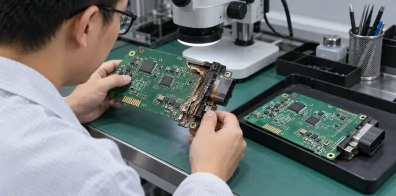
Board replacement is safer when repair cannot restore a stable mechanical interface, when the defect reaches the laminate or internal connection, or when the product’s approval system will not accept a repaired edge contact. Replacement also wins when a recurring connector fault will damage the repaired board again or when inspection costs approach the cost of a controlled rebuild.
Heat and arcing deserve a conservative response. Carbonized laminate can conduct and may extend beyond the visible mark. A discolored contact beside a melted slot can be the result of low contact force, misalignment, overload, contamination, or a loose system connection. Repairing the gold without correcting the cause leaves the highest-risk part of the failure in place.
| Decision factor | Repair remains plausible when | Replacement or rebuild is favored when |
|---|---|---|
| Damage depth | Contact surface or one replaceable land is affected | Laminate, internal copper, edge geometry, or several contacts are damaged |
| Mating system | Connector condition is verified and correctable | Slot damage or unknown contact force can repeat the failure |
| Product control | Drawing, contract, and approval authority allow the method | Critical application or customer control rejects repaired contacts |
| Verification | Thickness, geometry, resistance, mating, and function can be checked | The team cannot measure the property changed by the repair |
| Availability | Replacement is obsolete or has a long qualified lead time | Controlled fabrication data and a qualified replacement source exist |
| Lifecycle economics | One controlled repair restores useful service with low recurrence risk | Repeated repairs, downtime, inspection, and socket damage cost more |
Do not let sunk cost decide the disposition. An expensive board can still be unsafe to repair, while an obsolete low-volume board may justify a carefully controlled contact replacement. Record both the technical rejection criteria and the business comparison so the decision can be reviewed later.
How Should Repair vs Replacement Be Approved?
Engineering and quality should approve technical acceptability first. Purchasing and operations can then compare lead time, downtime, availability, and lifecycle cost among the technically acceptable options. This order prevents a fast or cheap repair from becoming the default before anyone proves that the board can be released.
Technical Disposition
The disposition should name the damage, repair method, governing drawing or deviation, product class or customer controls, technician qualification, required records, and acceptance tests. In a manufacturing setting, this may run through an MRB or nonconformance system. In field service, the title may differ, but someone still needs authority to accept the residual risk.
State what the repair will and will not restore. Under IPC terminology, a repair can restore functional capability without automatically proving full compliance with the original drawings. If the customer requires original-form compliance, the team needs a rework or replacement path that meets that requirement, or a written deviation. A vague note such as “cleaned and repaired” gives the next inspector no basis for release.
For a new build, a free PCB DFM check can confirm that the replacement data still supports the connector interface before tooling.
Cost and Downtime Decision
Compare more than the repair invoice. Include diagnosis, shipping, specialized labor, plating or bonding, inspection, functional test, production interruption, spare availability, connector replacement, and the cost of another failure. A board that returns in two days but fails after ten insertions may cost more than a controlled rebuild that takes longer.
Use an expected-service view. Estimate how long the repaired unit must remain in service, how many mating cycles it will see, whether a qualified spare exists, and whether replacement data is complete. If several identical boards show the same wear track, pause the batch decision and investigate the connector, assembly fixture, and original finish requirement. A repeat pattern changes the problem from one damaged board to a system corrective action.
An illustrative approval note can be brief and concrete: “One contact has shallow wear with intact nickel, no substrate damage, and a verified replacement socket. Approve selective nickel/gold plating to the drawing requirement. Release after thickness evidence, microscope review, four-wire comparison to two known-good contacts, five controlled mating cycles, and the system functional test.” Every clause points to an observable record.

How Do You Verify a Repaired Gold Finger?
Verify the repaired contact against the property changed by the work and the failure mode that started the investigation. A bright surface and continuity beep are incomplete evidence. The release package may need visual, dimensional, plating, bond, electrical, mating, and functional results.
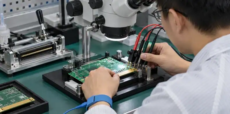
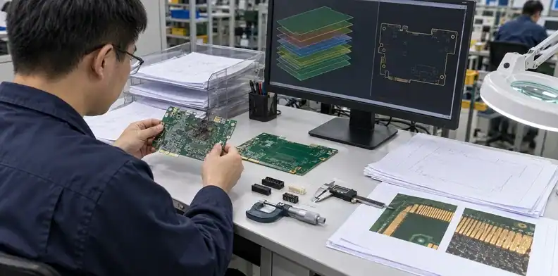
Use magnification to check alignment, spacing, edges, scratches, pits, discoloration, residue, and transition into the original conductor. Measure width, pitch, edge position, and bevel relationship when a replacement contact was installed. For replating, confirm the approved nickel and gold requirements using the specified method. If adhesion is part of the repair instruction, record that result without performing a destructive test that the product did not authorize.
Low-resistance measurements need a defined fixture and comparison. Four-wire sensing is useful when lead resistance would otherwise distort the result, but the value still depends on probe placement, contact force, surface condition, and temperature. Use the approved baseline. Then mate the board in a verified connector and reproduce the original electrical or functional condition. Movement, load, and temperature should be included when they were part of the failure.
| Verification layer | What to inspect or measure | Release evidence |
|---|---|---|
| Visual | Finish continuity, pits, scratches, residue, lift, heat damage | Before/after microscope images with affected contacts identified |
| Dimensional | Contact width, pitch, alignment, edge position, bevel relationship | Measurement record tied to drawing or approved deviation |
| Plating or bond | Nickel/gold evidence, coverage, adhesion or bonded-contact condition | Process traveler and thickness/bond inspection result |
| Electrical | Continuity plus approved low-resistance or signal check | Instrument, fixture, method, test points, baseline, result |
| Mechanical mating | Insertion fit, contact witness, retention, controlled cycles | Connector ID, cycle count, inspection after mating |
| Functional | Original symptom under relevant load, movement, and temperature | Pass/fail log with firmware/configuration and test conditions |
If a verification step cannot be performed, name the missing evidence and route the board back for disposition. Do not convert “not measured” into “passed.” The same record structure used for a formal failure analysis makes future recurrence easier to compare.
How Can You Prevent Repeat Damage?
Prevent repeat damage by correcting the whole mating interface. Inspect the slot or backplane contacts for contamination, bent springs, loss of contact force, debris, rough edges, and heat marks. Confirm that guides, brackets, ejectors, and enclosures align the card before the contacts engage. A repaired board inserted into a defective connector can fail on its first service cycle.
Control handling and storage. Hold the board by its edges, protect contacts in suitable ESD packaging, keep the mating face away from foam or tape residue, and define whether cleaning is allowed before incoming inspection. For field-replaceable cards, record insertion history when wear life matters. Replace worn sockets before they begin cutting the board finish.
On repeat orders, preserve the finish type, plating requirement, edge geometry, keepout, bevel callout, and inspection evidence in controlled data. Do not rely on a previous supplier’s memory or a golden sample without matching drawing notes. If a design change affects thickness, bevel, panelization, or contact length, review the connector interface again.
Use the evidence from the failure to choose the prevention action. Oil or residue calls for a handling or cleaning correction. A diagonal wear path points toward alignment. Uniform base-metal exposure across many fingers suggests finish or cycle-life review. One burned power contact calls for current, contact force, connector, and system checks before another board is installed.
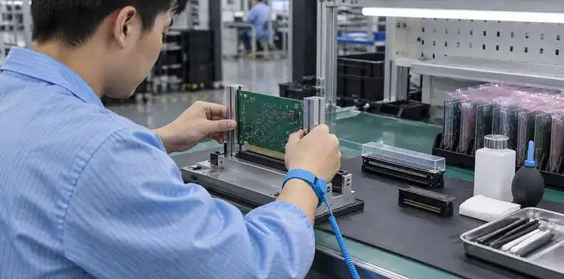
What Should You Send for a Replacement PCB Quote?
Send a replacement-board package that preserves the connector interface and removes the ambiguity that contributed to the failure. The manufacturer needs the controlled fabrication data, material and stackup, board thickness, finished outline, contact geometry, finish and thickness requirements, bevel detail, and inspection expectations. Failure photos and the disposition record explain what the new build must prevent.
Do not send only a damaged sample and ask the factory to copy it. Wear, repair, contamination, and board-edge loss can hide the original geometry. A sample can support fit review, but controlled digital data and an approved drawing should define the new board. If the old board is obsolete and files are incomplete, call that out so reverse engineering, connector measurement, and prototype qualification are quoted as separate work.
| RFQ item | What to include | Question it closes |
|---|---|---|
| Fabrication data | Gerber or ODB++, drill/rout data, netlist when available | What copper, mask, holes, and outline must be built? |
| Stackup and materials | Board thickness, laminate, copper, controlled impedance if applicable | Will the card fit and perform like the approved revision? |
| Gold-finger requirements | Contact drawing, hard-gold callout, nickel/gold requirement, masked area | What finish and wear surface must the factory produce? |
| Edge interface | Bevel angle/extent/stop, residual edge, connector datasheet or interface drawing | How will the card enter and mate without damage? |
| Inspection package | Visual class, thickness evidence, dimensions, electrical test, sample approval | What evidence releases the lot? |
| Failure and revision record | Photos, affected contacts, suspected cause, changes, approvers | What must change, and what must remain identical? |
| Commercial inputs | Quantity, prototype/production split, target date, shipping destination | What route, lead time, and price should be quoted? |
To compare another fabrication and assembly quote, you can also review Custom PCB Manufacturer — Fabrication & Assembly | PCBark. Send the same controlled drawing, connector interface, and acceptance requirements so the quotations are based on the same scope.
Ask the supplier to return CAM questions and any proposed changes in writing before tooling. A substitute finish, altered bevel, revised outline, or changed contact length needs the product owner’s approval. For files that are incomplete or uncertain, contact QueenEMS with the damaged-board photos and available fabrication package so the missing-data path can be scoped before quotation.
The most useful repair record ends with a prevention decision. If replacement is chosen, carry the verified connector, finish, and inspection requirements into the new revision so the next board does not inherit the same uncertainty.
FAQ
Can I use a pencil eraser to clean PCB gold fingers?
No. An eraser can remove contamination, but it can also abrade the gold, change the wear surface, leave particles, and hide the original damage pattern. Use an assembly-compatible cleaner and low-lint applicator under a controlled procedure, then inspect and retest the contact.
Can I repair a worn or missing gold finger with solder?
No. Solder is not a substitute for a flat, wear-resistant nickel-and-hard-gold contact surface. It changes geometry and hardness, can transfer material to the mating connector, and may create a raised edge. Worn plating needs a qualified selective-plating process; a missing contact needs an approved replacement-contact method or a new board.
How do I know whether the PCB or the mating connector caused the failure?
Compare the wear track with the connector position, inspect spring contacts and guides, record the failing slot, and repeat the electrical test with controlled known-good hardware when the product permits it. Diagonal scratches, damage concentrated at one edge, low contact force, or a failure that follows one slot point toward the connector or alignment system rather than the board alone.
Can a repaired gold finger return to a high-reliability product?
Yes—but only when the product drawing, contract, customer controls, and responsible approval authority allow the repair, and the finished contact passes the defined visual, dimensional, electrical, mating, and functional checks. A successful repair does not automatically prove full compliance with the original unmodified board requirements.
Sources
Written by the QueenEMS Engineering Team.
Upload your files today · Free DFM check before production · Ship worldwide
Get your PCB prototypes in as fast as 24 hours. We handle FR4, Rogers, and hybrid boards up to 40 layers in volume production, with advanced builds subject to engineering review — free prototypes for 2–4 layer FR-4 boards, no minimum order.
Just upload your Gerber + BOM — we source every part, assemble, and inspect (AOI + X‑Ray) so you don't have to chase suppliers. Boards ship in as fast as 24 hours.