
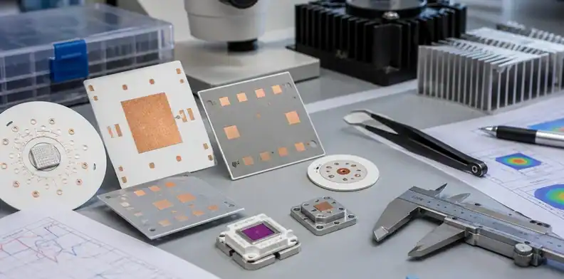
Quick Answer: A ceramic PCB for high-power LED projects should be selected by heat flux, wavelength exposure, package style, and assembly route. Alumina can fit many visible LED boards when the thermal load is moderate and cost matters; AlN becomes stronger when junction temperature, dense arrays, UV-C reliability, or compact heat-sink interfaces leave little thermal margin. The RFQ should state LED power, wavelength range, substrate material, copper process, finish, soldering exposure, optical/mechanical interface, and any reliability evidence required before the buyer compares price.
- High-power LED and UV-C boards should start with junction-temperature risk, not material preference.
- Alumina and AlN can both be valid, but they solve different cost, heat, and reliability problems.
- UV-C projects need extra attention to material exposure, package notes, cleanliness, and assembly documents.
High-power LED buyers often arrive with the same question: should this board be alumina ceramic, AlN ceramic, metal-core PCB, or something else? The answer changes when the LED is not just a lighting emitter but a dense array, UV-C source, curing head, optical module, or compact sealed product.
High-power visible LED and UV-C projects need a substrate decision that accounts for the complete thermal path, optical surfaces, attachment materials and operating conditions. The alumina versus AlN cost discussion provides related material-selection context; the project review should also establish the optical and assembly requirements.
Table of Contents
- What does a ceramic PCB solve in high-power LED designs?
- When is alumina enough for LED ceramic PCB?
- When should AlN replace alumina?
- What changes when the project is UV-C?
- How should copper, finish, and assembly affect the substrate choice?
- What evidence should an LED buyer request before ordering?
- How should overseas buyers choose the right LED ceramic PCB partner?
What does a ceramic PCB solve in high-power LED designs?
A ceramic PCB can provide an insulating heat path for a high-power LED assembly. The useful comparison is the temperature reached by the chosen package in the actual board, thermal interface and cooler. Ceramic is one candidate construction; increasing LED power does not create a universal point at which FR-4 or metal-core boards become unacceptable.
For low-power indicator boards, FR-4 or metal-core PCB may be enough. A high-power LED or UV-C emitter changes the risk profile. The board may sit close to a lens, reflector, quartz window, heat sink, seal, or enclosure wall. A small rise in thermal resistance can reduce optical output, accelerate lumen maintenance loss, shift wavelength behavior, or stress solder joints and wire bonds inside the LED package.
The buyer’s first task is to define the heat path. Name the LED package, drive current, expected board temperature, heat sink interface, operating duty cycle, and whether the board carries one emitter, a dense array, or a mixed LED and sensor layout. A supplier cannot select the right ceramic material from Gerbers alone when the thermal and optical load is missing.
Calculate junction temperature from the right reference point
For OSLON UV 3535, ams OSRAM AN155, dated 18 February 2026, section 2.3, uses Tj = Ts + IF × VF × RthJS,el. Ts is the solder-pad temperature under the LED; the resistance is the electrical-power-based value identified in the component data sheet. It is not the heat-sink temperature and not a material conductivity.
For an explicitly hypothetical arithmetic example, assume Ts = 60°C, IF = 0.35 A, VF = 6 V and RthJS,el = 10 K/W. The estimate is 60 + 0.35 × 6 × 10 = 81°C. These inputs are not ratings for a named LED, and 81°C is not a recommended operating target. Substitute the actual part’s values and the manufacturer’s specified temperature-measurement method.
The Cree LED thermal-management note, Rev. 5, also distinguishes the component-to-solder-point path from the board, thermal interface and heat sink. When comparing another manufacturer’s model, check whether its resistance is normalized to electrical input or dissipated heat. Subtracting optical output from power while retaining an electrical-power-based resistance mixes definitions. For an array, measure under the simultaneous loading, enclosure and airflow conditions used in service.
Ceramic substrates are useful because alumina and aluminum nitride both provide insulation, dimensional stability, and better heat handling than ordinary organic laminates. The choice between them is not a quality ranking. It is a fit decision based on heat, cost, layout density, assembly exposure, and reliability target.
When is alumina enough for LED ceramic PCB?
Alumina is often enough when the LED heat load is moderate, the board area gives enough spreading room, and the buyer needs a mature, cost-conscious ceramic route. It is a practical starting point for many visible LED modules, indicator arrays, lighting engines, and lower-density thermal boards where AlN would add cost without solving a proven bottleneck.
Start with the Ceramic PCB Guide to frame the material decision, then compare junction temperature, copper pattern, and the mounting path before selecting alumina or AlN.
Alumina can also be easier to source for common ceramic PCB geometries. Buyers may find more quoting options for standard thicknesses, laser-cut outlines, simple copper patterns, and small prototype lots. That matters when a startup or engineering team still needs fast DFM feedback, a sample set, or a build that includes assembly coordination rather than only bare substrate supply.
The warning sign is temperature margin. If the thermal model or bench test shows junction temperature close to the LED package limit, alumina may become the wrong economy. The cost saved on substrate material can disappear later through lower drive current, larger heat sinks, added thermal interface complexity, or product-life risk.
Use alumina when the design has enough area, the heat sink is realistic, the optical target allows moderate drive current, and the supplier can state the ceramic thickness, metallization route, copper thickness, surface finish, solderability, and inspection method. For a simple LED RFQ, that evidence is more useful than a broad claim that alumina is “good for LEDs.”
| Alumina fit signal | What the buyer should confirm |
|---|---|
| Moderate LED power density | Junction temperature has margin in the intended enclosure |
| Larger board or spreader area | The copper pattern and heat sink can actually move heat |
| Cost-sensitive prototype | The design is still proving optical and mechanical fit |
| Common visible LED module | No unusual UV-C exposure or severe reliability requirement |
Alumina is not a downgrade when it fits the thermal target. It is the wrong choice only when the board is being asked to carry heat, density, or exposure that it cannot support with margin.
When should AlN replace alumina?
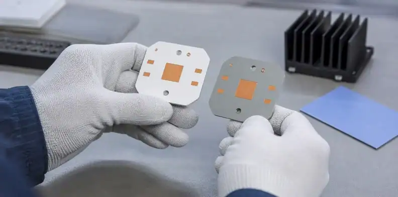
AlN should replace alumina when the thermal path is the limiting factor and the project cannot safely trade more board area, lower current, larger heat sink, or relaxed lifetime target. Kyocera describes AlN as having much higher thermal conductivity than alumina and positions it for high heat-dissipation package and substrate use, which is the reason buyers review it for dense LED and UV-C designs.
The most common trigger is a dense LED array. When emitters sit close together, local hot spots become more important than average board temperature. AlN can help pull heat away from small source areas faster, which may reduce thermal gradients and protect optical output stability.
Another trigger is mechanical packaging. Some products do not have room for a larger metal-core PCB, extra copper area, or a bigger heat sink. UV disinfection modules, compact curing heads, optical sensing devices, and sealed industrial products often force the thermal design into a smaller space. In that case, the substrate may need to do more work.
A hot array center with an apparently cool heat sink is a useful reason to investigate before ordering AlN. In an illustrative LED build, measure the specified solder-point temperature near the center and an outer emitter, then record temperatures at accessible points along the board-to-sink path. Run the intended emitter combination at the same current and allow the readings to stabilize. A cool sink alone cannot distinguish limited spreading in the board from poor contact beneath it.
Check the interface coverage and assembled gap against the mounting specification. If that contact is suspect, evaluate a corrected interface on the existing ceramic first. If the contact meets its requirement and the remaining temperature margin is inadequate, compare a feasible AlN construction with the alumina baseline using equivalent attachment and cooling. Record any unavoidable thickness or metallization difference as part of the comparison. Verify solder-point temperature and optical output at the required operating condition; a lower surface temperature is not an LED lifetime result. The useful outcome is a demonstrated thermal gap that the proposed construction closes, rather than a material upgrade selected from the heat-sink reading alone.
| AlN trigger | Why it matters in LED/UV-C sourcing |
|---|---|
| Dense emitter array | Reduces heat-spreading pressure around local hot spots |
| Compact heat sink | Helps when the board must transfer heat through a small contact area |
| Higher drive current | Preserves thermal margin when optical output is pushed |
| UV-C reliability target | Supports tighter thermal control in a harsh optical environment |
| Failed alumina prototype | Gives a controlled next option instead of guessing at fixes |
For broader material background, use the QueenEMS ceramic PCB manufacturer hub. For this LED decision, the useful RFQ phrase is narrower: “Quote alumina and AlN options only if each option includes material grade, copper route, finish, and thermal/assembly assumptions.”
What changes when the project is UV-C?
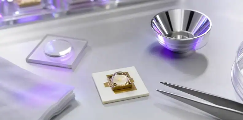
UV-C projects add exposure and documentation risks that ordinary visible LED boards may not have. The ceramic substrate still needs to move heat, but the buyer must also check wavelength range, package handling notes, optical window or lens materials, cleanliness, solder mask exposure, adhesive exposure, and whether nearby materials are compatible with UV-C radiation.
UV-C LEDs are used in air, water, surface treatment, curing, sensing, and other applications where optical power and lifetime depend heavily on thermal and material control. Nichia describes UV LED portfolios across UV-A, UV-B, and UV-C wavelength ranges, while ams OSRAM’s OSLON UV application material emphasizes handling, processing, and solder pad design for UV-C LED products. Those supplier notes matter because the ceramic PCB is only one part of a larger optical and thermal assembly.
The OSLON UV application note, sections 2.4 and 3.4, links optical stability to chemical compatibility and cautions against wet cleaning these non-hermetic LED products. This is a product-family restriction; it should be checked before choosing a post-assembly wash merely because the bare ceramic tolerates that liquid. Follow the actual LED package guidance for a different component.
| Exposure zone | What to identify | Useful verification |
|---|---|---|
| Direct or reflected UV | Wavelength, irradiance at the material and duty cycle | Material-specific UV-aging or optical data at relevant exposure |
| Nearby adhesives/coatings/inks | Exact product, cure state and location | Compatibility with the LED, optics and enclosure environment |
| Exposed metal or finish | Finish stack, contact with air/moisture and optical role | Solderability and any required spectral reflectance/aging evidence |
| Cleaning path | Solvent, temperature and access to package openings | Component-approved cleaning route and representative assembly check |
Record the illuminated area on the assembly drawing. A material shielded behind the substrate faces a different exposure from one beside the emitter window. Bare-metal reflectivity, ceramic color and a visible-light photograph do not establish UV-C reflectance or stability. Where the optical design depends on those properties, request data at the intended wavelength instead of assuming a bright surface is suitable.
Buyers should send the LED package datasheet, wavelength, optical output target, duty cycle, heat sink drawing, enclosure material, window or lens material, and cleaning requirement with the RFQ. The supplier should return a quote that separates board manufacturing assumptions from LED package handling assumptions. If the quote only says “ceramic PCB for UV-C” with no material, finish, or assembly notes, the risk is still hidden.
How should copper, finish, and assembly affect the substrate choice?
Copper, surface finish, and assembly exposure can change the practical choice between alumina and AlN. A substrate with the right ceramic material can still fail the project if the copper pattern, solder pad finish, flatness, or assembly process is not controlled.
Start with copper thickness and geometry. LED boards often need broad copper pads, thermal spreading areas, and clean current paths. Dense arrays may also need tight spacing, consistent pad registration, and predictable solder wetting. Ask whether the supplier is quoting DPC, thick film, direct copper, or another ceramic metallization route, because each route changes copper thickness, line/space limits, adhesion, cost, and surface finish options.
Surface finish should follow the LED package and assembly process. ENIG, immersion silver, OSP-like routes, or other finishes may have different solderability and storage assumptions depending on the supplier’s process. The buyer should request the finish recommendation tied to the LED package, solder alloy, reflow profile, and any wire bonding or eutectic attachment requirement.
Assembly exposure matters because ceramic boards are rigid and brittle compared with organic laminates. Panel handling, pick-and-place support, stencil design, reflow ramp, heat sink attachment torque, and cleaning method can all affect yield. The quote should name whether QueenEMS or another partner is responsible for bare board only, PCB plus assembly, or a controlled handoff to the buyer’s assembler.
| RFQ item | Why it changes the LED ceramic PCB decision |
|---|---|
| Copper process | Defines thickness, adhesion, pattern limits, and thermal spreading |
| Surface finish | Controls solderability, LED package compatibility, and storage risk |
| Reflow profile | Shows whether the ceramic and metallization route match assembly heat |
| Heat sink interface | Determines flatness, mounting pressure, and thermal contact risk |
| Cleaning method | Matters for UV-C optics and contamination-sensitive emitters |
For first builds, pair this article with the QueenEMS guide on ordering your first ceramic PCB prototype. The prototype file package should include more than Gerbers when LEDs, optics, and heat sinks are involved.
What evidence should an LED buyer request before ordering?
Before ordering, the buyer should request evidence that matches the LED risk: material statement, process route, copper and finish details, dimensional inspection, solderability or assembly notes, thermal assumptions, and packaging controls. For UV-C, add handling, cleanliness, and optical-material exposure notes.
A practical LED ceramic PCB quote should state the ceramic family, finished thickness, copper thickness, metallization route, surface finish, outline tolerance, hole or slot details, and whether the design is reviewed as bare board or assembled PCBA. If the LED will be mounted by the supplier, the quote should also reference BOM/AVL, LED package orientation, paste type, stencil thickness, reflow profile, polarity marking, and inspection method.
The best evidence depends on project maturity. A prototype may only need DFM notes, material alternatives, and a controlled sample build. A production release should need drawing revision control, inspection records, material traceability, packaging labels, and change-control rules. UV-C production may need extra records for cleaning, handling, optical-window protection, and storage.
| Evidence to request | Prototype stage | Production stage |
|---|---|---|
| Material/process statement | Required | Locked to drawing revision |
| Copper/finish detail | Required | Controlled by approved spec |
| Assembly notes | Needed if LEDs are mounted | Reflow and inspection records required |
| Thermal assumption | Engineering estimate acceptable | Test condition should be recorded |
| UV-C handling notes | Required for UV-C | Required with packaging and cleaning records |
A supplier that can quote only the substrate may still be useful for material supply. A buyer who needs a working LED module, however, often needs DFM feedback, assembly coordination, and documentation in the same conversation. That is a different supplier fit.
How should overseas buyers choose the right LED ceramic PCB partner?
Select the LED project partner according to the deliverable and development stage. A material specialist may be right for bare alumina or AlN substrate supply; an LED package house may be right for emitter selection; a PCB/PCBA partner is more useful when the buyer needs a prototype, assembly review, English DFM feedback, and a controlled quote package.
For a first LED or UV-C build, prioritize communication speed and question quality. A useful supplier will ask about LED package, wavelength, drive current, heat sink, enclosure, optics, surface finish, assembly scope, and inspection records. A weak answer will quote “ceramic PCB” from Gerbers without asking what thermal or UV exposure the board must survive.
For repeat production, the same partner must control documents. The drawing should freeze substrate material, copper process, finish, outline tolerance, LED placement, polarity marks, heat-sink interface, packaging, and change-control rules. Purchasing should not substitute alumina for AlN, or one finish for another, without engineering approval.
QueenEMS fits projects where the buyer needs practical RFQ support rather than only a material catalog answer. For a high-power LED or UV-C module, that can mean reviewing whether alumina or AlN is the right quoting path, checking missing thermal and assembly inputs, coordinating PCB fabrication and PCBA when needed, and returning English DFM questions for overseas teams.
FAQ
Is alumina ceramic PCB good enough for high-power LED?
Yes, alumina can be good enough when LED power density is moderate, the heat sink has margin, and the design is not constrained by severe size or lifetime targets. Use AlN only when the thermal model, bench test, or package requirement shows that alumina lacks margin.
Is AlN always better for UV-C LED boards?
No. AlN can improve thermal control, which is valuable for UV-C, but UV-C reliability also depends on package handling, optics, finishes, adhesives, cleanliness, and enclosure materials. A good RFQ checks the full exposure path.
Can I use metal-core PCB instead of ceramic PCB for LED?
Sometimes. Metal-core PCB can fit many LED lighting products, especially when electrical insulation and thermal resistance are acceptable. Ceramic PCB becomes more attractive when higher insulation, compact heat spreading, UV-C exposure, or ceramic package compatibility matters.
What should I send for a ceramic PCB LED quote?
Send Gerber or ODB++ files, fabrication drawing, LED package datasheet, BOM, drive current, wavelength for UV projects, heat sink drawing, target substrate material if known, copper/finish preference, assembly scope, quantity, and reliability evidence needs.
How do I compare alumina and AlN quotes fairly?
Compare the same drawing, copper route, finish, thickness, assembly scope, inspection records, and delivery quantity. A lower alumina price is not comparable to an AlN quote if the thermal target, finish, or assembly boundary is different.
Send QueenEMS a high-power LED or UV-C ceramic PCB RFQ
Submit the LED data sheet, drive condition, wavelength, circuit drawing, thermal interface, optics and cleaning constraints through the QueenEMS LED project contact. Include the required quantity and assembly responsibility. The response should identify the proposed substrate and finish, plus any missing thermal or optical input that prevents a meaningful comparison.
Sources
- Kyocera, Aluminum Nitride (AlN) Packages / Substrates
- ams OSRAM, OSLON UV details on properties, handling, and processing
Written by the QueenEMS Engineering Team
Upload your files today · Free DFM check before production · Ship worldwide
Get your PCB prototypes in as fast as 24 hours. We handle FR4, Rogers, and Flex up to 60 layers — free prototypes for 2–4 layer boards, no minimum order.
Just upload your Gerber + BOM — we source every part, assemble, and inspect (AOI + X‑Ray) so you don't have to chase suppliers. Boards ship in as fast as 24 hours.