

Quick Answer: PCB fabrication for harsh environments starts with a quantified mission profile, then matches laminate, stack-up, copper, vias, surface finish, cleanliness, protection, and qualification evidence to the actual stresses. High Tg material, heavy copper, or conformal coating can each solve a specific problem, but none is a universal ruggedization package. Release the build only after the fabrication drawing, assembly protection plan, and environmental tests address the same temperature, moisture, chemical, vibration, and service conditions.
“Harsh environment” is too broad for a material callout. A board beside a hot motor, a sensor exposed to condensation, and an outdoor controller near salt spray can all fail for different reasons. If they receive the same generic “high-reliability PCB” note, the supplier must either guess or quote unnecessary controls.
The sourcing task is to convert field exposure into measurable requirements. Bare-board fabrication controls the substrate, stack-up, plated structures, finish, geometry, cleanliness-related design inputs, and fabrication evidence. Assembly and product engineering control components, solder joints, coating or potting, enclosure, mounting, and system-level validation. The boundaries must meet, but they should not be confused.
Table of Contents
- Start with the mission profile, not a material
- Match laminate properties to thermal stress
- Control moisture and contamination paths
- Design copper and vias for cyclic strain
- Choose a finish for the exposure and assembly
- Mechanical loads require board and enclosure work
- Coating and potting are separate process decisions
- Qualification must reproduce the real failure mode
- Control substitutions throughout the product life
- Write a harsh-environment PCB RFQ
Start with the mission profile, not a material
A specification for pcb fabrication for harsh environments starts with a mission profile: the conditions the electronics will experience, for how long, in which operating state, and with what acceptable consequence. It turns words such as hot, humid, vibrating, dusty, or corrosive into engineering inputs.
Define exposure and operating state
Record ambient and local temperatures, power state, duty cycle, rate of change, humidity and condensation, contaminants, pressure or altitude where relevant, vibration spectrum, mechanical shock, electrical transients, radiation if applicable, cleaning agents, expected life, service access, and storage or transport conditions. Include enclosure class, airflow, mounting points, and cable loads because the board does not experience the environment in isolation.
| Mission-profile input | Useful description | Weak description |
|---|---|---|
| Temperature | Operating, non-operating, local hot spot, cycle rate | “High temperature” |
| Moisture | Humidity range, condensation, immersion, salt, duration | “Waterproof PCB” |
| Chemicals | Named fluid, concentration, splash/vapor, cleaning method | “Chemical resistant” |
| Mechanical load | Spectrum, axes, mounting, shock pulse, board mass | “High vibration” |
| Product life | Cycles, operating hours, service interval, failure consequence | “Long life” |
Separate continuous limits from excursions
A short assembly reflow exposure, a one-hour transport cold soak, and ten years of powered service at elevated temperature are different stresses. Material datasheets and component ratings often use different test conditions, so copy-pasting one temperature number into the drawing can create a false safety margin.
Define normal operation, worst credible operation, non-operating storage, transport, assembly processing, and abnormal excursions separately. The design team should own the product requirement; the fabricator should confirm that the proposed board construction and process can meet it.
If the mission profile is incomplete, request a pre-RFQ assessment with the enclosure, load locations, environmental test plan, and proposed stack-up. The useful output is a list of missing inputs and risk-driving assumptions, not a generic recommendation for “rugged material.”

Match laminate properties to thermal stress
Choose the laminate system from the thermal, mechanical, electrical, flammability, and fabrication requirements together. A high glass-transition temperature (Tg) can be relevant, but Tg alone does not prove performance under a mission profile.
Tg alone does not define suitability
Tg identifies a change in polymer behavior under the stated test method. Harsh-environment reliability can also depend on coefficient of thermal expansion (CTE), decomposition behavior, moisture absorption, peel strength, dielectric properties, resin content, copper adhesion, and compatibility with the required number of thermal cycles.
The stack-up converts those properties into a board. Dielectric thickness, copper distribution, plated-hole geometry, board size, and mounting can create stress even when the material name looks suitable. Ask the supplier to connect the proposed laminate and prepreg set to the finished construction rather than approving a brand family in isolation.
| Thermal problem | Property or construction to examine | Evidence before release |
|---|---|---|
| Repeated temperature cycling | CTE relationships, plated-hole structure, copper ductility | Stack-up review and representative cycling plan |
| High continuous ambient | Material capability at time and temperature | Datasheet plus system thermal analysis |
| Local power hot spot | Copper spreading, vias, interface, enclosure path | Thermal model or instrumented prototype |
| Assembly thermal exposure | Laminate cure, moisture, finish, component process | Approved reflow/assembly profile |
| Wide board temperature gradient | Stack symmetry, mounting, copper balance | Flatness and mechanical review |
Use a controlled PCB material substitution process because a change made for availability can alter CTE, resin flow, loss, flammability documentation, or lamination compensation. “Equivalent high Tg” is not a complete approval criterion.

Control moisture and contamination paths
Moisture becomes dangerous when it reaches conductive surfaces, residues, damaged interfaces, or biased spacing where corrosion and leakage can progress. The design needs a barrier strategy, but it also needs cleanliness, drainage, material, spacing, and enclosure decisions that prevent the barrier from hiding contamination.
Condensation deserves separate attention from high humidity. A product can meet a steady humidity condition and still collect water when its temperature crosses the local dew point. Connector entries, enclosure seams, pressure changes, cable wicking, and cold surfaces can direct moisture to one location even when most of the assembly stays dry.
| Threat path | Bare-board control | Assembly or product control |
|---|---|---|
| Surface leakage | Adequate spacing and finish condition | Clean assembly and coating where justified |
| Corrosion at exposed metal | Compatible surface finish and drawing notes | Enclosure, gasket, coating, connector selection |
| Conductive residue | Fabrication cleanliness and protected packaging | Flux/process cleanliness verification |
| Trapped condensation | Layout that avoids water traps where possible | Drainage, venting, thermal and enclosure design |
| Chemical attack | Compatible laminate, mask, finish, legend | Qualified coating, seals, and material compatibility |
The PCB ionic-cleanliness evidence should be specified only at the stage and method that answer the product risk. Bare-board residues and assembled-board residues are not the same measurement problem. A clean bare PCB can still be contaminated during soldering, cleaning, handling, or coating.
Surface spacing also remains a design responsibility. Conformal coating can change the environmental protection strategy, but it should not be used casually to justify inadequate uncoated geometry. The approval record should state which acceptance rules assume coating and what happens at masked connectors, test points, edges, and rework locations.

Design copper and vias for cyclic strain
Copper thickness and plated structures should be chosen for current, thermal, fabrication, and fatigue requirements rather than as a general symbol of ruggedness. More copper helps some problems and can worsen resin fill, etching, balance, weight, or strain in others.
Copper weight solves only the right problem
Use conductor calculations, voltage-drop limits, temperature-rise targets, short-circuit conditions, and heat-spreading needs to select copper. The heavy-copper PCB design guide is relevant when the power path supports the choice. It does not prove vibration resistance or moisture survival by itself.
Thick external copper can require wider spacing and different etch compensation. Uneven copper distribution can contribute to board movement. High-current neck-downs at pads, vias, fuses, or connectors may remain the limiting section even if broad planes use heavier copper.
Via evidence belongs in the qualification plan
Thermal cycling loads plated-through holes because copper, resin, and glass do not expand identically. The risk depends on the laminate system, board thickness, hole diameter, aspect ratio, plating, inner-layer connection, resin condition, and cycle profile. Microvias, blind vias, filled structures, and stacked arrangements introduce different mechanisms and should not inherit a through-hole conclusion.
State finished hole size, plating requirement, via structure, acceptance basis, and any coupon or microsection sampling. The PCB microsection report review helps define what a cross-section can demonstrate and why one sample does not describe every board automatically.

Choose a finish for the exposure and assembly
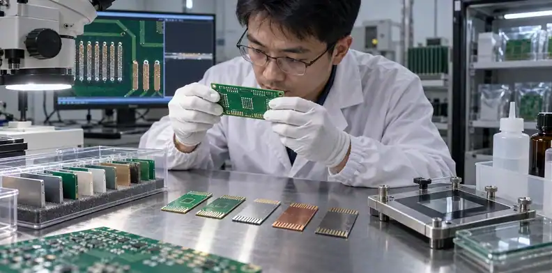
Surface finish must support soldering or contact function while remaining compatible with storage, handling, environmental exposure, coating, and the selected assembly process. No finish makes the entire assembly corrosion-proof.
For fine-pitch assembly, confirm whether the land pattern requires a planar finish and prove it with an assembly trial. Repeated mating, edge contacts, or wire bonding need local finish drawings and thickness evidence. Storage and logistics require a shelf-life, packaging, and solderability plan. Coating or potting adds a mask drawing and adhesion check, while a chemical environment requires compatibility testing with the named agents.
Compare specific options rather than labeling one “high reliability.” The PCB surface-finish thickness requirements matter when plating thickness or local contact performance is acceptance-critical. Ordinary solderable pads and repeated mating contacts may need different local treatments.
Finish selection also affects repair. Some assemblies will be serviced, connectors replaced, or test points probed. Define which surfaces may be touched, cleaned, recoated, or reworked without invalidating the environmental protection plan.
Finally, control packaging and handling. A correct finish can still arrive damaged or contaminated if boards rub, absorb moisture, or remain open in an uncontrolled environment before assembly. Receiving should inspect package condition, labels, lot identity, surface appearance, and any required shelf-life evidence.
Mechanical loads require board and enclosure work
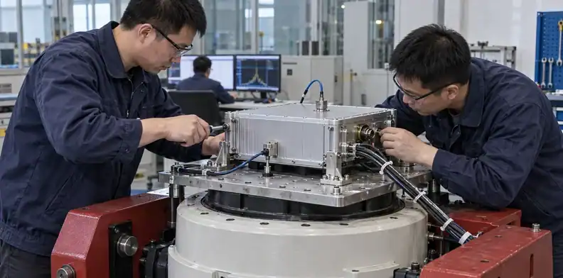
Vibration and shock are system loads transmitted through mounting points, connectors, cables, components, and the enclosure. A thicker PCB or a flexible material may help in a particular mode, but neither is a universal mechanical solution.
Board fabrication cannot fix unsupported mass
Map board supports, unsupported spans, heavy components, tall components, edge connectors, cable forces, and resonant modes. A rigid board with poorly placed supports can flex around a connector. A flex circuit can remove a connector yet fail at a sharp transition or unrestrained dynamic bend. A stiffener can support an interface while transferring stress to its edge.
Mounting-hole keep-outs, washer areas, grounding hardware, press-fit connectors, card guides, and chassis contact need coordinated drawings. Mechanical hardware should not crush copper, cut mask, distort the board, or depend on uncontrolled board thickness. The completed assembly should be tested in its intended orientation and enclosure because fixture-only board testing may miss system resonances.
Signal integrity can also change under the mechanical solution. Long cable paths, shields, chassis bonds, and connector transitions may alter return current or noise coupling. Use the controlled-impedance PCB requirements when the interface truly needs controlled geometry, then verify that mounting and environmental controls do not break the reference path.
The procurement boundary is clear: the PCB fabricator can confirm board construction and dimensional evidence, while the product owner must approve the enclosure, supports, fasteners, cable loads, component retention, and system test.
Coating and potting are separate process decisions
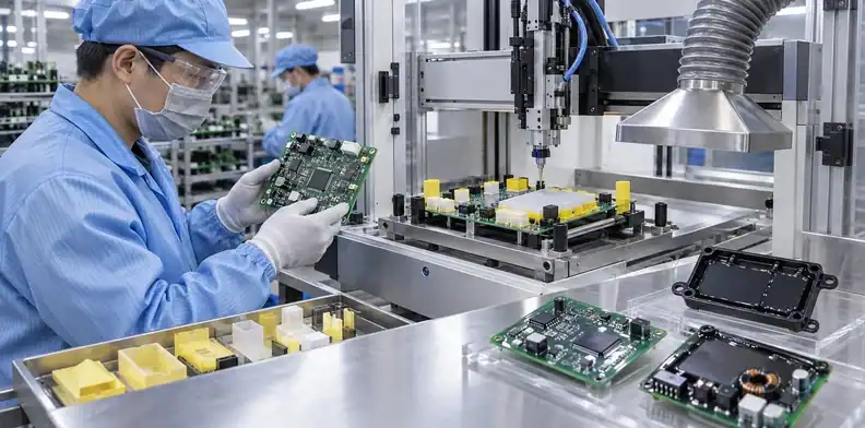
Conformal coating and potting protect an assembled board, so they must be specified with assembly cleanliness, masking, coverage, cure, inspection, repair, and material compatibility. They are not bare-board finishes and should not be implied by a request for a “harsh-environment PCB.”
Cleanliness comes before coating
Coating over contamination can trap residues and moisture against the surface. Define the soldering and cleaning process, cleanliness verification, handling window, and maximum delay before coating. If no-clean flux is used, confirm compatibility through evidence rather than assuming its residue is harmless under every coating and bias condition.
IPC-CC-830 establishes qualification and conformance requirements for electrical insulating compounds used as conformal coatings. Material qualification does not by itself define application workmanship, local coverage, masking, cure, or product-specific environmental performance.
Connectors, test points, heatsink interfaces, switches, sensors, adjustment points, grounding contacts, and mechanical mating surfaces may need masking. The drawing should define keep-out boundaries and the allowed transition rather than relying on an operator’s interpretation.
Potting provides a different level of encapsulation and changes heat flow, mass, reworkability, stress, and inspection. A soft protective gel, rigid epoxy, silicone, or urethane system can behave differently around components and under temperature cycling. Select it as part of the product mechanical and thermal design.
The conformal-coating type decision can support that assembly review. The final selection still needs compatibility with the actual laminate, mask, legend, finish, components, flux residues, enclosure, and field chemicals.
Qualification must reproduce the real failure mode
Environmental testing is useful only when the specimen, fixture, operating state, severity, duration, and acceptance criteria represent the product risk. Passing an unrelated test can create confidence without covering the mechanism that causes field failure.
| Risk | Representative evidence | Acceptance must define |
|---|---|---|
| Thermal cycling | Powered or unpowered cycling with relevant dwell/ramp | Function, resistance, inspection, sample size |
| Damp heat or condensation | Controlled humidity/temperature and bias state | Leakage, corrosion, insulation, visual criteria |
| Vibration or shock | Product mounting, axes, spectrum/pulse | Function during/after, hardware and solder inspection |
| Chemical exposure | Named agent, concentration, temperature, duration | Swelling, adhesion, corrosion, electrical performance |
| Combined environment | Sequenced or simultaneous stresses where justified | Order, recovery, retest, failure analysis |
An illustrative example is a sensor PCB that passes steady high-humidity storage but fails after daily cold starts. Investigation should not jump directly to a new laminate. The symptom suggests condensation during temperature transition, so the team should inspect the enclosure path, residue locations, connector entry, high-impedance nodes, coating coverage, and powered state. A revised test would cycle through the dew-point condition with the assembly biased, then measure leakage and inspect corrosion-prone areas. A material or coating change is justified only after that mechanism is supported.
This is a worked scenario, not a QueenEMS field claim. It shows why the action and verification method must follow the failure condition.
Document preconditioning, board revision, material lot, assembly process, coating or potting lot, fixture, test profile, failures, rework, and retest. A pass/fail summary without configuration control cannot support a future repeat order.

Control substitutions throughout the product life
A rugged design can lose its qualification basis when material, finish, solder mask, copper foil, prepreg, coating, component, or process changes without review. The approved product record should distinguish locked items from properties that may be met by an equivalent.
Require an approval boundary for material changes
For each controlled item, state the exact part or material, critical properties, acceptable alternates, notification requirement, evidence needed, and approver. A blanket “no substitutions” note can create unnecessary supply risk; an unlimited “equivalent allowed” note can erase the qualification basis.
Changes should be evaluated against the failure mechanisms, not only the drawing title. A laminate replacement may affect CTE and plated-hole cycling. A finish change may affect soldering, coating adhesion, or contact behavior. A mask change may affect chemical resistance. A coating change may require new cure and compatibility evidence.
Keep prototype and production traceability. Lot, date code, material identity, traveler, test reports, deviations, and approval correspondence should connect the delivered boards to the agreed construction. The PCB quality-document package helps define which records belong at shipment instead of after a field problem.
For repeat orders, review changes to the product environment as well. A new enclosure, higher power firmware mode, different cleaning agent, relocated cable, or longer storage period may invalidate an unchanged PCB qualification.

Write a harsh-environment PCB RFQ
The RFQ should connect each exposure to a construction decision and a verification method. This allows suppliers to quote the same risk rather than interpreting “rugged PCB” in different ways.
| RFQ section | Required input | Expected supplier response |
|---|---|---|
| Mission profile | Temperature, moisture, chemicals, vibration, life, enclosure | Assumptions and uncovered risks |
| Board construction | Stack-up, material rule, copper, vias, thickness, finish | Proposed controlled construction |
| Assembly protection | Cleaning, coating/potting, masking, cure, repair | Process scope and exclusions |
| Qualification | Test profiles, specimen state, acceptance, samples | Method, reporting, and exceptions |
| Change control | Locked items, equivalency boundary, notice | Traceability and approval process |
| Commercial scope | Prototype/production quantities and delivery | Comparable quote and validation stages |
Reference standards by revision and purpose. Do not assume that a high performance class automatically selects the laminate, coating, enclosure, or environmental test. Likewise, a coating qualification does not certify a complete assembly for a field condition.
Close the DFM and evidence plan before ordering production material. The DFM review before purchase order should identify every unresolved material, stack-up, clearance, finish, test, coating, or mechanical item and name the approval owner.
To price the build against its mission profile, provide QueenEMS with the fabrication drawing, stack-up, controlled material list, enclosure and mounting data, coating or potting scope, qualification profiles, acceptance criteria, and quantity stages. The response can return a quote-readiness review, proposed fabrication boundary, open DFM questions, and the evidence needed before prototype or production release.

FAQ
Is high-Tg FR-4 enough for every harsh environment?
No. Tg addresses one material transition, while the product may also depend on CTE, moisture, chemicals, vibration, copper geometry, vias, components, coating, enclosure, and the actual temperature-time profile.
Does heavy copper make a PCB more vibration-resistant?
Not automatically. Copper thickness should follow current and thermal needs. Vibration reliability also depends on board geometry, mounting, component mass, connectors, solder joints, stiffeners, and enclosure behavior.
Is conformal coating applied during PCB fabrication?
Usually no. It is normally an assembly-level process applied after components are soldered and the assembly is cleaned or otherwise prepared under a qualified process.
Which test should I request for a rugged PCB?
Request the test that reproduces the credible failure mechanism, with the actual assembly state, mounting, operating condition, severity, duration, and acceptance criteria defined.
Can an equivalent laminate be used after qualification?
Only within the approved change-control boundary. Compare the properties and failure mechanisms that supported qualification, then document the evidence and approval before use.
Sources
- IPC-6012: Qualification and Performance Specification for Rigid Printed Boards
- IPC-CC-830: Qualification and Performance of Electrical Insulating Compounds
Written by the QueenEMS Engineering Team
Upload your files today · Free DFM check before production · Ship worldwide
Get your PCB prototypes in as fast as 24 hours. We handle FR4, Rogers, and hybrid boards up to 40 layers in volume production, with advanced builds subject to engineering review — free prototypes for 2–4 layer FR-4 boards, no minimum order.
Just upload your Gerber + BOM — we source every part, assemble, and inspect (AOI + X‑Ray) so you don't have to chase suppliers. Boards ship in as fast as 24 hours.