
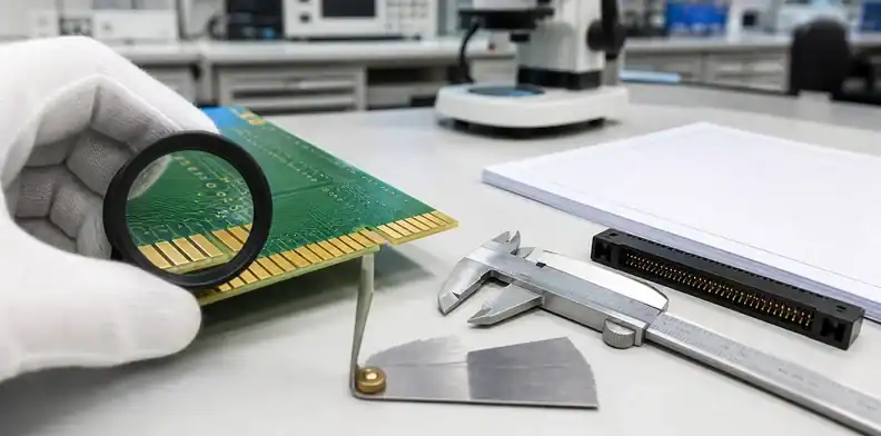
Quick Answer: PCB gold finger plating acceptance should define the plated contact area, hard-gold requirement, bevel, nickel barrier, thickness evidence, cosmetic limits, and mating-zone inspection. Buyers should separate ordinary ENIG pads from wear-contact fingers because the quotation and acceptance evidence are different.
PCB gold finger plating problems are expensive because they appear at the product interface: card edge fit, insertion wear, exposed nickel, burrs, scratches, or finish thickness evidence that does not cover the contact zone. This page does not replace a finish-selection comparison. It helps buyers send a quote package that tells the supplier exactly which contact fingers are controlled and what proof belongs with the shipment.
Table of Contents
- What should the gold finger drawing control?
- When should hard gold be separated from ENIG?
- How do bevel and outline tolerance affect mating?
- What thickness evidence should be requested?
- Which defects should pause acceptance?
- How should masking and selective plating be approved?
- How should repeat orders protect the same edge finish?
- What should QueenEMS receive for gold finger review?
- How should buyers prevent gold finger disputes?
What should the gold finger drawing control?
The drawing should control the finger area, plating type, bevel requirement, keepout from solder mask, contact length, edge tolerance, and any cosmetic acceptance limit in the mating zone. A finish note that only says gold plated edge is not enough for quotation.
For the broader contact discussion, see PCB gold fingers for reliable mating. This RFQ page focuses on what the buyer must freeze before the supplier prices hard-gold processing.
Drawing rule: define the contact zone as a controlled mechanical and finish feature.
When should hard gold be separated from ENIG?
Hard gold should be separated from ENIG whenever the edge contact experiences repeated insertion, wiping, or mechanical wear. ENIG may be suitable for solderable pads, but it should not be silently applied to an edge connector that needs wear resistance.
Use ENIG versus hard gold selection for the finish choice. In the RFQ, list which features receive hard gold and which pads keep ENIG, HASL, OSP, or another finish.
Finish boundary: do not let one finish name cover both solder pads and wear contacts.
| Interface need | Better finish callout | RFQ evidence to request |
|---|---|---|
| Repeated connector insertion | Hard gold on the finger area | Thickness report and contact-zone photo |
| General solder pads | ENIG or the board finish already selected | Normal finish evidence, not a finger report |
| Mixed contact and solder areas | Selective hard gold plus separate pad finish | Drawing map that names each controlled region |
How do bevel and outline tolerance affect mating?
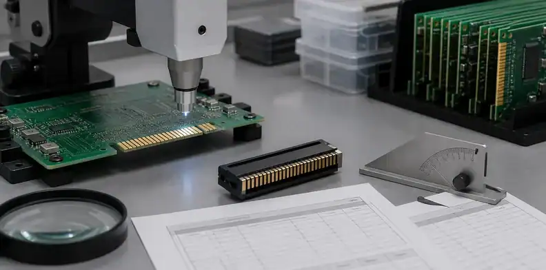
Bevel angle, bevel depth, board thickness, and outline tolerance decide whether the card edge enters the connector smoothly. A plating system can be correct while the board still fails because the edge is rough, oversized, or beveled inconsistently.
Pair the finger note with PCB board outline tolerance when the connector slot has little mechanical margin. The supplier needs the finished edge target before routing and beveling are treated as routine.
Fit signal: gold finger acceptance includes the edge geometry, not only the metal stack.
What thickness evidence should be requested?
Ask for finish thickness evidence that covers the controlled contact area. A generic surface-finish certificate may not prove the finger zone if the report measures only standard pads or unrelated locations.
The surface finish thickness evidence page explains how buyers should read finish reports. For gold fingers, the report should identify the measured feature or a representative rule tied to the contact area.
Proof rule: the report should prove the finger plating, not just the board’s general finish.
Which defects should pause acceptance?
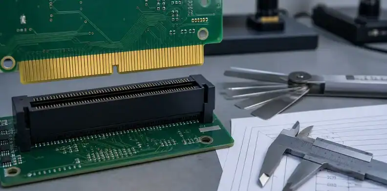
Pause acceptance when the mating zone shows scratches through plating, exposed copper or nickel, burrs, contamination, mask encroachment, severe nicks, poor bevel quality, or plating that does not match the agreed evidence. Minor cosmetic marks outside the contact zone should be judged by the drawing and class requirement.
Receiving can use PCB incoming inspection as the general workflow, but gold fingers deserve a feature-specific check because they are handled and worn differently from solder pads.
Receiving call: inspect the actual mating path before releasing the lot to assembly.
| Observation | Likely risk | Buyer response |
|---|---|---|
| Exposed copper at the edge | Connector wear or corrosion concern | Hold release until supplier explains disposition |
| Tab mark near wipe area | Mechanical or cosmetic contact concern | Compare with connector contact length |
| Scratches outside contact area | Usually lower risk | Record as cosmetic unless the drawing says otherwise |
How should masking and selective plating be approved?
Selective plating needs a clear boundary. The RFQ should state where hard gold starts and stops, whether nearby pads have a different finish, and whether exposed traces or mask gaps near the finger edge are acceptable.
Supplier CAM may propose mask or plating adjustments to make selective processing stable. Those changes should be marked because they can affect connector clearance, solderable pads, or cosmetic appearance.
CAM boundary: selective plating edits need visual approval when they touch the contact zone or nearby pads.
How should repeat orders protect the same edge finish?
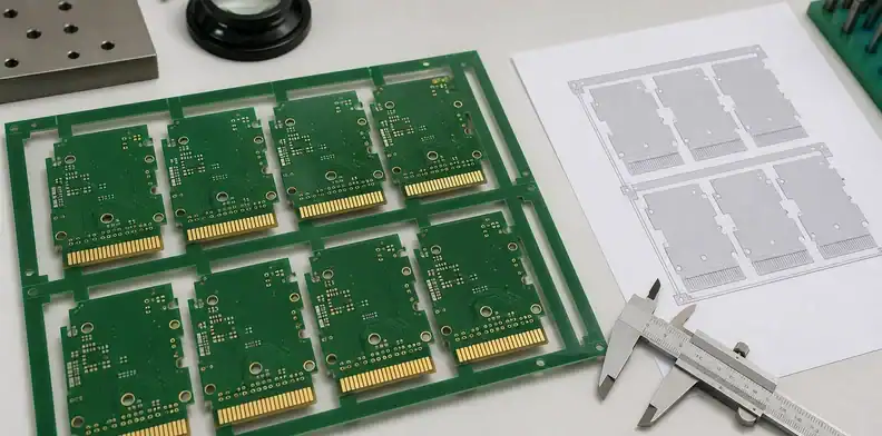
Keep the accepted plating note, thickness evidence rule, bevel requirement, and connector fit assumption with the product revision. Repeat orders can drift when a buyer copies only Gerbers and forgets the earlier finish clarification.
A second supplier should receive the same contact-zone map and evidence expectation. That makes the quote comparable and reduces the chance that one supplier quotes ENIG where another quotes hard gold.
Repeat rule: archive the contact-zone decision, not only the final order price.
What should QueenEMS receive for gold finger review?
QueenEMS should receive fabrication data, edge connector drawing, board thickness target, bevel note, finish callout, required thickness evidence, quantity, and any connector fit constraint. Send those details through the QueenEMS contact page so the review can identify finish conflicts, edge tolerance questions, and evidence needed before quotation.
A useful supplier response should return the hard-gold area, finish assumptions, bevel method, report scope, and any CAM change before production release.
RFQ close: make the mating zone the center of the quote, not an afterthought in the finish note.
How should buyers prevent gold finger disputes?
Gold finger disputes are easiest to prevent before the supplier starts selective plating. The buyer should define the connector interface, insertion expectation, hard-gold area, bevel, board thickness, masking boundary, thickness evidence, and receiving inspection rule in one release package. If those items are scattered across emails, the finished edge becomes difficult to judge.
A practical RFQ sentence is: “Gold fingers are controlled contact features. Quote hard gold on the marked mating area, include bevel and finished board thickness assumptions, provide finish thickness evidence for the finger area or agreed representative feature, and report any mask, plating, or edge-geometry change before CAM approval.” That gives both purchasing and quality a clear acceptance basis.
Supplier replies should be checked for finish language. “Gold finish” can mean several things in a quotation, and a supplier may quote ENIG unless the hard-gold area is explicit. Ask the supplier to separate solderable pads from mating contacts and confirm which finish applies to each area. This is especially important when the board has ENIG pads and hard-gold fingers on the same part.
Bevel approval deserves its own line. The connector may require a bevel for insertion, but the PCB drawing may only show the outline. Ask the supplier to confirm bevel angle, edge quality, and whether beveling affects the plated contact length. If the supplier cannot confirm the connector requirement, engineering should review the mechanical drawing before release.
Thickness evidence should be tied to the contact feature. A report that measures a general pad may not represent a selectively plated finger. Ask how the supplier selects measurement points and whether the report identifies the controlled area. The buyer does not need to inspect the plating bath, but the buyer needs evidence that the functional contact zone was controlled.
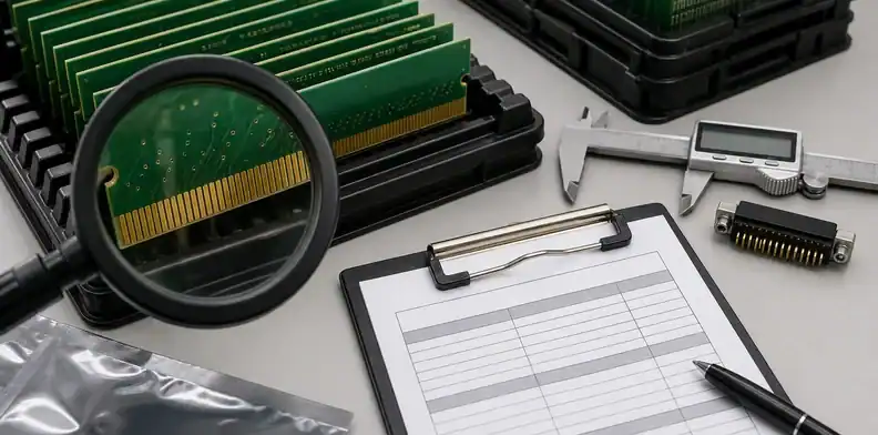
Visual acceptance should distinguish the mating zone from the rest of the board. Small handling marks on a nonfunctional rail are not the same as scratches, exposed nickel, or burrs on the wiping path. Receiving inspection should look at the connector-facing edge under enough magnification to make a defensible decision.
Packaging can also matter. Gold fingers should not arrive scratched by panel scrap, loose hardware, or abrasive separators. If the board has exposed contacts, ask for packaging that protects the edge and keeps the contact area clean. The acceptance plan should not assume that a good plated edge survives poor handling.
For repeat orders, store the accepted edge photograph, finish report format, bevel note, and connector requirement. When a later buyer changes supplier or asks for cost reduction, that record shows which details are functional. It also keeps a future quote from replacing a controlled hard-gold area with a cheaper finish by accident.
If a supplier proposes a change, require a marked before/after view. A shorter plating area, different bevel, mask pullback, or altered outline tolerance can all change connector fit. Approve those changes as engineering decisions, not as informal shop-floor optimizations.
The buyer should also define whether cosmetic appearance is customer-facing. Some card edges are hidden inside a connector and judged mainly by function. Others are visible during service, testing, or customer inspection. Cosmetic expectations can affect handling, packaging, and acceptance, so they should be separated from electrical wear requirements.
For shipment evidence, ask for a finish report, feature photos when the contact zone is critical, and confirmation that the bevel and edge were inspected. Do not ask for a large document package if the contact is low duty and low risk. Evidence should match the insertion and customer-acceptance requirement.
A gold finger issue should have a disposition path. If the report is missing but the boards look good, can the supplier provide the report before assembly? If scratches appear on the contact zone, does engineering accept a concession or require remake? If bevel is wrong, can the board be used in a different fixture, or is the lot blocked? These questions should be answered before the boards are urgently needed.
Assembly teams should know whether cleaning, masking, or handling restrictions apply to the fingers. Fingerprints, abrasive separators, or rough trays can create avoidable contact problems after fabrication. If the product has a sensitive connector, packaging and handling become part of the acceptance plan.
For second sourcing, compare not only gold thickness but also selective plating method, bevel capability, edge routing, and report format. A new supplier may quote the same words but deliver a different contact edge. Ask for a first article when the connector interface controls product reliability.
The final release package should let a buyer inspect the lot without interpreting plating terminology from scratch. It should show the contact map, finish requirement, bevel note, evidence rule, packaging expectation, and approval owner for any finish substitution.
A buyer should also decide whether sample mating is required before production. For a new connector, a first article can be inserted into the mating socket to confirm thickness, bevel, and contact position. That test is not a substitute for plating evidence, but it catches mechanical mismatch that a finish report cannot show.
If the supplier proposes a different bevel or contact length, compare it against the connector drawing. Some changes are harmless because the wiping zone remains covered. Others shorten the usable contact or expose laminate at the entry edge. A marked edge view makes the decision much faster.
For receiving, keep one accepted photo of the contact zone. It gives quality and purchasing a visual reference for scratches, burrs, discoloration, and bevel condition. The photo does not replace the drawing, but it prevents every lot from becoming a fresh interpretation of what a good gold finger looks like.
A final quote package should also state whether the finger edge can be panelized with breakaway tabs nearby. Tabs too close to the contact zone can leave marks or handling risk. The supplier should show where the part is held during processing when the contact zone is customer-critical.
If the product uses a keyed connector, include the keying or chamfer geometry with the edge drawing. A perfect plating report will not save a board that enters the connector incorrectly. Mechanical fit and plating evidence should be reviewed as one contact-interface package.
When a buyer receives a supplier exception, the response should name the impact: finish evidence only, bevel geometry, board thickness, cosmetic appearance, or connector fit. This keeps a minor plating paperwork issue from being confused with a real mating failure risk.
If the connector supplier provides a mating specification, attach it or summarize the controlled values. Card thickness, bevel, insertion direction, contact length, and wear expectation may all be defined outside the PCB drawing. The fabricator can then quote the gold finger as a connector interface instead of a decorative finish.
For production lots, decide whether every shipment needs a finish thickness report or whether first-lot evidence plus supplier process control is enough. Customer-facing products, high insertion count, or warranty-sensitive contacts usually deserve stronger evidence. Low-duty programming fingers may not need the same package. The RFQ should make that distinction visible before price comparison.
Receiving inspection should connect the plating evidence to the connector zone, not only to the surface finish name. A report can confirm that gold was applied while still leaving questions about bevel location, exposed copper at the edge, tab witness marks, or cosmetic scratches in the wipe area. Buyers should define which conditions are functional rejects and which are cosmetic observations that do not affect the mating interface.
The supplier response should also separate prototype flexibility from production release. During EVT or DVT, engineering may accept extra photos, manual measurement, or a one-time process note while the connector choice is still being tuned. Once the connector and card edge are frozen, the quote should move to a repeatable acceptance package so the same questions do not reopen on every purchase order.
FAQ
Can ENIG be used for gold fingers?
Sometimes for low-wear contacts, but repeated insertion normally needs a hard-gold contact finish approved for the mating requirement. The RFQ should state whether the edge is a wear contact or only a low-duty exposed pad.
Do gold fingers always need beveling?
Most card-edge connectors expect a beveled edge, but the drawing or connector requirement should define the target. Do not let the fabricator guess the bevel when the connector fit is controlled.
Where should thickness be measured?
At the controlled finger area or a representative feature agreed before production, not only on unrelated solder pads. The report should make the measurement basis clear enough for receiving inspection.
Sources
- IPC, IPC-4552B Specification for Electroless Nickel/Immersion Gold
- IPC, IPC-6012 Qualification and Performance Specification for Rigid Printed Boards
Written by the QueenEMS Engineering Team
Upload your files today · Free DFM check before production · Ship worldwide
Get your PCB prototypes in as fast as 24 hours. We handle FR4, Rogers, and hybrid boards up to 40 layers in volume production, with advanced builds subject to engineering review — free prototypes for 2–4 layer FR-4 boards, no minimum order.
Just upload your Gerber + BOM — we source every part, assemble, and inspect (AOI + X‑Ray) so you don't have to chase suppliers. Boards ship in as fast as 24 hours.