
Quick Answer: ENIG costs $0.50–$1.00 per square inch and offers the best solderability for fine-pitch surface mount devices, while hard gold costs $1.50–$3.00 and survives 1,000+ insertion cycles for edge connectors. Soft gold, running $2.00–$4.00 per square inch, is strictly required for reliable wire bonding because its 20–100μin pure gold thickness provides necessary wire adhesion. Key takeaways:
- ENIG limits gold thickness to 0.05–0.10μm to prevent brittle solder joints during assembly.
- Hard gold utilizes a cobalt or nickel alloy to reach an extreme 130–200 Knoop hardness.
- Soft gold features ≥99.9% purity specifically designed for Chip-on-Board (COB) wire bonding.
- Combining all three finishes on one board adds $0.50–$1.00 and 3–5 production days.
Table of Contents
- What Is the Real Difference Between ENIG, Hard Gold, and Soft Gold?
- How Does Each PCB Gold Finish Process Work?
- Which Gold Finish Delivers the Best Solderability?
- How Do Durability and Wear Resistance Compare Across All Three?
- What Does Each Gold Finish Actually Cost Per Board?
- When Does Black Pad Risk Make ENIG the Wrong Choice?
- Which Finish Should You Specify for Edge Connectors?
- When Do You Need Soft Gold for Wire Bonding Applications?
- Can You Combine Multiple Gold Finishes on One PCB?
- How Should Your Fab Drawing Specify the Right Gold Finish?
Hardware engineers frequently face costly field failures when specifying the wrong gold finish for their printed circuit boards. Choosing an incorrect plating causes embrittled solder joints that snap under thermal stress or edge connectors that wear through their protective layers prematurely. By understanding the mechanical limits and exact costs of ENIG vs Hard Gold vs Soft Gold, you can prevent these critical defects. While reading a standard HASL vs ENIG surface finish comparison helps for basic boards, high-reliability applications require knowing precisely when to upgrade to electrolytic gold.
What Is the Real Difference Between ENIG, Hard Gold, and Soft Gold?
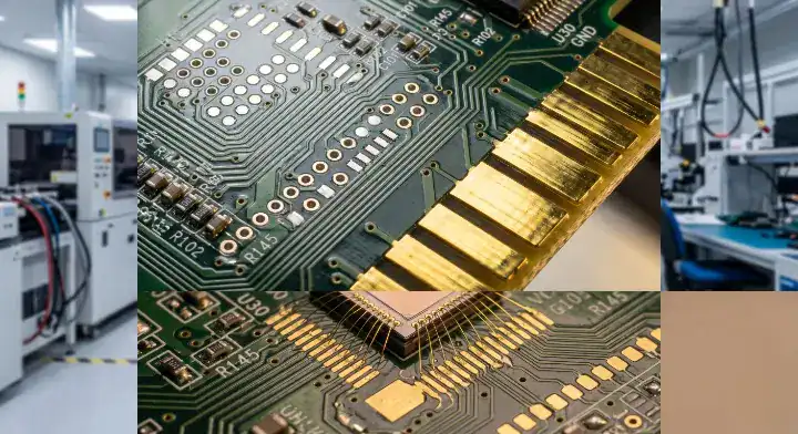
ENIG is a chemically deposited finish containing 3–6μm of nickel and 0.05–0.1μm of pure gold, whereas hard gold and soft gold are electrolytically plated finishes requiring physical electrical connections. Hard gold adds cobalt to achieve high mechanical durability, while soft gold maintains 99.9% purity to facilitate wire bonding.
Electroless Nickel Immersion Gold (ENIG) is a flat, solderable surface finish deposited via chemical reaction. It typically costs $0.50–$1.00 per square inch. Because it requires no electrical bus lines, manufacturers can apply it evenly to high-density boards with isolated traces.
Here is the reality: Electrolytic processes deposit much thicker gold layers but fundamentally change the material’s physical properties.
- ENIG provides the flattest surface for fine-pitch components.
- Hard gold resists heavy sliding friction.
- Soft gold deforms slightly under pressure to grab bonding wires.
| Finish Type | Application Method | Purity Level | Typical Thickness |
|---|---|---|---|
| ENIG | Chemical deposition | Pure Gold | 0.05–0.1μm |
| Hard Gold | Electrolytic plating | Alloyed (Cobalt/Nickel) | 0.75–1.25μm |
| Soft Gold | Electrolytic plating | ≥99.9% Pure Gold | 0.5–2.5μm |
Choose ENIG if your board primarily features surface mount components requiring highly planar pads. Choose hard gold if your design includes edge connectors that will be repeatedly inserted into slots.
Bottom line: Specify ENIG for standard component assembly, but switch to selective electrolytic gold only when mechanical friction or direct die wire bonding is required.
How Does Each PCB Gold Finish Process Work?
The ENIG process uses an autocatalytic chemical reaction to deposit nickel, followed by a displacement reaction for gold, requiring no electrical connections. Conversely, electrolytic hard and soft gold require a plating bus to apply an electrical current through a chemical bath, which deposits thicker gold layers up to 100μin.
Because electrolytic plating requires all target pads to be electrically connected during the plating phase, manufacturers must route temporary bus traces that are later removed or isolated. This makes full-board electrolytic plating nearly impossible for modern, high-density interconnect (HDI) designs.
Think about this: Chemical deposition coats everything exposed, while electrolytic plating only coats what is electrically charged.
- ENIG tanks submerge the entire panel for uniform chemical coating.
- Electrolytic plating requires precise mask alignment for selective areas.
- Flash gold is a very thin electrolytic pre-plate often misleadingly sold as true hard gold.
| Process Characteristic | ENIG | Hard/Soft Gold (Electrolytic) |
|---|---|---|
| Electrical Bus Required | No | Yes |
| Plating Location | Entire exposed copper | Selectively masked areas |
| Setup Complexity | Moderate | High |
Choose the chemical ENIG process if your board features hundreds of unconnected component pads. Choose the electrolytic process if you only need heavy gold on specific, easily routed outer-layer features like connector fingers.
Bottom line: Rely on ENIG for the bulk of your board’s surface finish to avoid routing impossible plating bus networks, using electrolytic methods strictly as secondary, selective processes.
Which Gold Finish Delivers the Best Solderability?
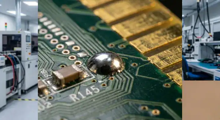
ENIG delivers the highest solderability because its thin 0.05–0.10μm pure gold layer dissolves rapidly into the solder, preventing the formation of brittle intermetallic compounds (IMC). Hard gold causes brittle solder joints because its cobalt alloy and excessive thickness easily push the solder joint’s gold content above the critical 3 wt% failure threshold.
Many engineers on Epec and PCBgogo forums report massive headaches with manual soldering and brittle joint failures when trying to mount components on hard gold pads. Because hard gold is highly alloyed, it does not wet easily with standard solder pastes. If you are reviewing a BGA pad design and assembly guide, you will see that pure immersion gold guarantees the strongest metallurgical bond with the underlying nickel.
Keep in mind: Gold embrittlement is a silent killer that causes joints to crack months after passing electrical tests.
- ENIG gold completely dissolves, leaving the solder to bond with the nickel.
- Hard gold’s cobalt impurities contaminate the solder pool.
- Exceeding 3 wt% gold in any solder joint guarantees brittle AuSn failure.
| Finish Type | Solder Wetting | Embrittlement Risk |
|---|---|---|
| ENIG | Excellent | Very Low |
| Soft Gold | Good | Moderate (due to thickness) |
| Hard Gold | Poor | Extreme |
Choose ENIG if your primary assembly method is reflow soldering for SMDs and BGAs. Avoid hard gold completely if any component needs to be soldered to that specific pad.
Bottom line: Never specify hard gold on SMT pads; always use ENIG to ensure strong, reliable solder joints that avoid catastrophic gold embrittlement.
How Do Durability and Wear Resistance Compare Across All Three?
Hard gold dominates wear resistance with a hardness of 130–200 Knoop, easily surviving over 1,000 insertion cycles on heavily used edge connectors. Soft gold offers only 60–85 Knoop hardness, and ENIG wears through completely to the nickel base in fewer than 50 mechanical insertions.
Hard gold is an electrolytic gold-cobalt alloy engineered specifically for mechanical toughness. It handles the severe sliding friction of PCIe slots and memory sockets. In contrast, soft gold relies on extreme purity, making it ductile and highly susceptible to scratching.
The truth is: Using the wrong gold finish on a wear surface guarantees rapid oxidation and signal failure.
- ENIG protects against oxidation but provides zero mechanical wear resistance.
- Soft gold’s ductile nature makes it perfect for wire deformation, not friction.
- Hard gold’s alloy structure acts as a rigid armor for copper pads.
| Finish Type | Hardness (Knoop) | Max Insertion Cycles | Shelf Life |
|---|---|---|---|
| Hard Gold | 130–200 | 1,000+ | 24+ months |
| Soft Gold | 60–85 | < 100 | 6–12 months |
| ENIG | N/A (Too thin) | < 50 | 12–18 months |
Choose hard gold if your product requires repeated physical plugging into sockets. Choose soft gold or ENIG if the pads will simply be sealed inside an enclosure after assembly.
Bottom line: Hard gold is the absolute only acceptable finish for sliding contacts and edge connectors due to its specific cobalt-hardened alloy structure.
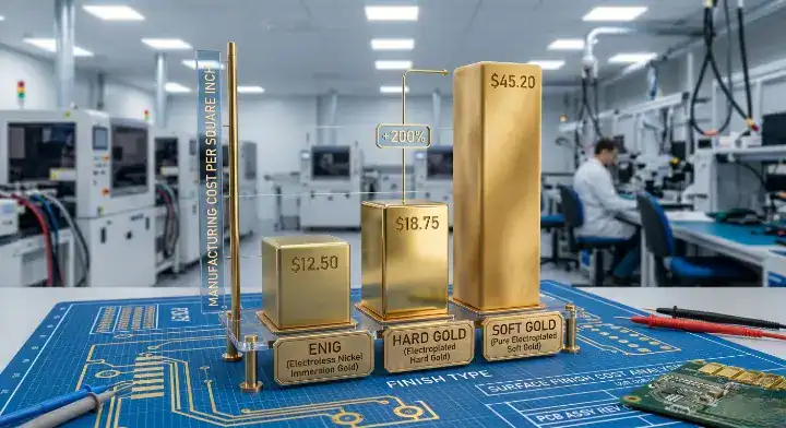
What Does Each Gold Finish Actually Cost Per Board?
ENIG is the most economical at $0.50–$1.00 per square inch, while hard gold ranges from $1.50–$3.00 per square inch depending on the plated area. Soft gold is the most expensive finish, costing $2.00–$4.00 per square inch due to the massive volume of pure gold required to achieve its 20–100μin thickness.
Because ENIG is an autocatalytic batch process, it coats all exposed copper simultaneously, making it highly efficient for mass production. Selective electrolytic plating requires expensive photolithography masking steps to ensure the gold only deposits on specific fingers or bonding zones.
What you should know: High material costs and extra processing days make electrolytic gold a premium feature.
- ENIG serves as the baseline cost for premium RoHS-compliant boards.
- Selective hard gold masking requires high alignment precision, slightly impacting yields.
- Soft gold consumes the highest actual volume of precious metal.
| Finish Type | Cost Per Sq. Inch | Processing Time Impact |
|---|---|---|
| ENIG | $0.50–$1.00 | Standard |
| Hard Gold | $1.50–$3.00 | + 1 to 2 days |
| Soft Gold | $2.00–$4.00 | + 2 to 3 days |
For prototype runs (5–10 boards), expect ENIG to be included in standard quick-turn pricing. For high-volume production (1,000+ boards), expect selective hard gold to add noticeable unit costs, requiring strict pad area minimization.
Bottom line: Minimize your use of electrolytic gold to strictly the specific pads that need it, using ENIG for the remaining 95% of the board to heavily control costs.
When Does Black Pad Risk Make ENIG the Wrong Choice?
Black pad occurs on ENIG boards when the immersion gold bath excessively corrodes the underlying nickel layer, causing catastrophic solder joint failures, especially on pads larger than 10mm. Preventing this requires strictly controlling the nickel bath’s phosphorus content between 7–9 wt% per the IPC-4552B standard.
Engineers on SMTnet and finishing.com frequently battle mysterious BGA failures linked to black pad. The root cause is a poorly maintained nickel bath that experiences extended exposure times during the gold displacement reaction. If you are actively preventing black pad defects on ENIG boards, you know that IPC-4552B introduced statistical sampling to replace outdated single-point rejection methods, giving engineers better batch visibility.
At QueenEMS, we track every ENIG bath cycle with real-time monitoring of nickel phosphorus content. A client shipped us 200 panels for BGA assembly, and during our incoming inspection, XRF measurements on the actual BGA pads showed gold thickness at 0.12μm—exceeding the IPC-4552B maximum of 0.10μm. The coupon measurements from the fabricator showed 0.08μm, which would have falsely passed. We rejected the batch and required re-plating, because excess gold thickness directly causes gold embrittlement. After re-plating to 0.07μm, the boards passed our 3X reflow reliability test with zero joint failures across 1,200 BGA solder balls.
This is critical: Relying on test coupons instead of measuring the actual board pads leads to false confidence.
- Black pad risk increases exponentially on large surface area pads.
- Phosphorus content must remain locked between 7–9%.
- XRF measurements must be taken on real application pads.
| Defect Risk | Root Cause | Prevention Strategy |
|---|---|---|
| Black Pad | Nickel corrosion during gold deposition | Maintain 7-9% phosphorus |
| Gold Embrittlement | Gold thickness > 0.10μm | Strict immersion bath timing |
| Poor Wetting | Contaminated gold bath | Daily chemical titration |
Choose an ENIG factory that provides statistical XRF reports on real pads if you are mounting high-value BGAs. Avoid cheap fabricators that only measure outer-rail test coupons.
Bottom line: Demand actual pad XRF measurements rather than test coupon data from your fabricator to accurately prevent black pad corrosion and gold embrittlement.
Which Finish Should You Specify for Edge Connectors?
You must specify hard gold plating at a minimum thickness of 30μin (0.76μm) for edge connectors to meet the IPC-4556 standard. This specific thickness, combined with the cobalt alloy, guarantees reliable electrical conductivity and physical integrity even after 1,000 insertion cycles.
When designing memory modules or PCIe interfaces, a standard PCB gold fingers plating guide will warn you that anything less than 30μin wears out rapidly. The electrolytic plating process forces the gold-cobalt alloy deep into the nickel base, creating an incredibly resilient shield.
Make no mistake: Attempting to cut costs by using ENIG on an edge connector will result in immediate field returns.
- IPC-4556 requires 130–200 Knoop hardness.
- Fingers must be beveled to reduce insertion friction.
- Plating bus traces must be routed to every single finger and later severed.
| Application Type | Recommended Finish | Reason |
|---|---|---|
| PCIe / RAM Edge Connectors | Hard Gold (30μin+) | Survives 1000+ insertions |
| Flat Flex Cable (FFC) Contacts | Hard Gold (15-30μin) | Resists sliding wear |
| Static Test Points | ENIG | Low friction, highly solderable |
Choose 30μin hard gold if your device will be plugged and unplugged by end-users constantly. Choose 15μin hard gold if it is an internal connector that will only be mated a few times during factory assembly.
Bottom line: Always call out IPC-4556 compliant hard gold for PCIe cards, RAM sticks, and any board-to-board edge connector experiencing sliding friction.
When Do You Need Soft Gold for Wire Bonding Applications?
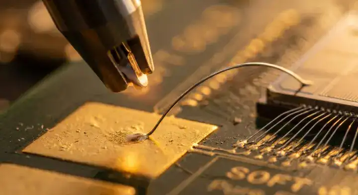
Soft gold is mandatory for Chip-on-Board (COB) and BGA substrates because its 15–100μin thickness of 99.9% pure gold provides the necessary deformation for strong aluminum or gold wire bonds. ENIG’s maximum gold thickness of 5μin is far too thin, resulting in immediate wire bonding adhesion failures.
Engineers on mpe.researchmfg.com frequently ask why their aluminum wires fail pull tests on standard ENIG boards. Because ENIG tops out at roughly 4μin of gold, the ultrasonic bonding tool punches straight through to the hard nickel, destroying the bond. Wire bonding requires a soft, thick cushion of pure metal to deform and weld properly.
Pay close attention: Specifying the wrong gold purity for wire bonding wastes thousands of dollars in ruined silicon dies.
- Soft gold electrolytic plating easily achieves 15–100μin thicknesses.
- A typical COB spec is 25μin pure gold over 150–200μin nickel.
- CMOS image sensors rely heavily on soft gold wire bonding.
| Wire Material | Minimum Gold Thickness | Recommended Finish |
|---|---|---|
| Aluminum Wire | 15–25 μin | Electrolytic Soft Gold |
| Gold Wire | 30–50 μin | Electrolytic Soft Gold |
| Not Applicable | 2–4 μin | ENIG (Soldering only) |
Choose soft gold electrolytic plating if you are doing bare die attachment and ultrasonic wire bonding. Choose ENIG only if you are soldering standard packaged components.
Bottom line: Specify electrolytic soft gold at a minimum of 25μin over 150μin of nickel whenever your design includes direct bare die wire bonding.
Can You Combine Multiple Gold Finishes on One PCB?
Yes, you can combine ENIG, hard gold, and soft gold on a single PCB, typically adding $0.50–$1.00 per board and 3–5 days to your production lead time. The process requires selectively plating the electrolytic hard and soft gold before applying the solder mask, followed by the ENIG chemical deposition afterward.
A robotics startup recently needed a 10-layer HDI board featuring fine-pitch BGA packages (0.4mm pitch), a COB wire bonding area, and a 60-pin edge connector seeing 500+ insertion cycles during dev testing. We used ENIG on all standard SMT pads for reliable soldering, selective soft gold (25μin pure gold over 150μin nickel) on the wire bonding area, and hard gold (30μin per IPC-4556) on the edge connector fingers. This triple-finish approach added $0.85 per board and 5 extra production days versus ENIG-only. However, it delivered 800+ connector insertion cycles, a 100% wire bond pull test pass rate, and a 99.8% first-pass yield on BGA assembly—meeting all three conflicting requirements on a single board.
Here is the catch: Multiple finishes require highly accurate photolithography masking, increasing the minimum order quantity (MOQ) considerations due to setup complexity.
- Electrolytic finishes (hard/soft) must be applied first.
- Solder mask is applied to protect the electrolytic gold.
- ENIG chemistry is applied last to the remaining exposed copper.
| Feature on Board | Assigned Finish | Expected Lead Time Impact |
|---|---|---|
| Only SMT Components | ENIG Only | Standard |
| SMT + Edge Connector | ENIG + Selective Hard Gold | + 2 Days |
| SMT + Connector + COB | ENIG + Hard + Soft Gold | + 5 Days |
Choose a hybrid ENIG and hard gold finish if your board has both fine-pitch BGAs and high-wear edge connectors. Choose the triple-finish approach only for complex aerospace or advanced sensory boards.
Bottom line: Do not compromise on reliability; pay the minor cost and time premium for hybrid finishes to ensure every pad performs its specific mechanical or electrical function perfectly.
How Should Your Fab Drawing Specify the Right Gold Finish?
Your fabrication drawing must explicitly call out the finish type, required thickness ranges, and applicable IPC standards, rather than simply writing ambiguous terms like “Gold Plating.” For example, specifying “ENIG per IPC-4552B, Au 0.05-0.10μm” ensures the manufacturer applies the exact chemical process required for assembly success.
Using our rapid PCB prototyping services allows you to test different finish thickness variations before committing to high-volume production. We provide a Free DFM/DFA engineering review on every order to catch missing IPC callouts before manufacturing begins.
Remember this: Vague fab notes give cheap manufacturers the loophole they need to apply flash gold instead of true hard gold.
- Always cite IPC-4552B for ENIG requirements.
- Always cite IPC-4556 for edge connector fingers.
- Provide a dedicated Gerber layer identifying selective electrolytic plating zones.
| Fab Note Requirement | Correct Example | Incorrect Example |
|---|---|---|
| Thickness | Au 0.76μm minimum | Thick gold |
| Standard | Per IPC-4556 | Industry standard |
| Process | Electrolytic Hard Gold | Gold plate |
Choose to write exhaustive fab notes if you want guaranteed reliability across multiple production batches. Avoid single-sentence finish descriptions that leave the chemistry choice up to the factory operator.
Bottom line: Explicitly detail your finish requirements, thicknesses, and selective plating zones on your fab drawings to eliminate manufacturing ambiguity and prevent costly rework.
Navigating the complexities of surface finishes determines whether your hardware survives the field or fails instantly during assembly. By keeping ENIG restricted to highly planar soldered components, leveraging hard gold for friction-heavy connectors, and isolating soft gold for precise wire bonding, you optimize both your budget and your reliability. At QueenEMS, we run up to 60-layer PCB fabrication with full turnkey service, ensuring your hybrid surface finishes are executed flawlessly. Contact us today to have our engineering team review your Gerber files and recommend the perfect, cost-optimized gold finish strategy for your next production run.
Written by the QueenEMS Engineering Team
FAQ
Can I use ENIG for wire bonding instead of soft gold? No, unless you are strictly doing aluminum wire bonding on small pads where the gold thickness naturally reaches at least 3-5μin. For gold wire bonding or high-reliability applications like COB and BGA substrates, you need electrolytic soft gold at 20-100μin thickness because ENIG’s maximum of 5μin doesn’t provide enough physical adhesion for consistent bond strength. Check your die attach specifications immediately.
What’s the best gold finish for PCB edge connectors? Hard gold at 30-50μin thickness per IPC-4556 is the absolute best choice. Hard gold’s cobalt or nickel alloy creates a surface hardness of 130-200 Knoop that withstands 1000+ sliding insertion cycles. ENIG wears through in under 50 cycles, and soft gold is too ductile for repeated friction. Specify selective hard gold on your fab drawing today.
How do I know if black pad will affect my ENIG boards? Demand nickel bath phosphorus content reports (which must be 7-9 wt%) and XRF thickness measurements taken on actual pads, not test coupons. Black pad risk increases exponentially with larger pad sizes above 10mm and with poorly controlled factory nickel baths. IPC-4552B provides the statistical sampling framework for your incoming inspection. Request our IPC-4552B compliance report for your next batch.
Can I put three different gold finishes on one PCB? Yes. A common configuration is ENIG on SMT pads, hard gold on edge connectors, and soft gold on wire bonding areas. The process sequence matters: electrolytic gold (hard and soft) is plated before the solder mask, and then ENIG is applied after the solder mask. Expect 3-5 extra days and $0.50-$1.00 additional cost per board. Send us your design for a custom hybrid plating quote.
How much more does hard gold cost compared to ENIG? Hard gold runs $1.50-$3.00 per square inch versus a baseline of $0.50-$1.00 for ENIG. Soft gold is the most expensive at $2.00-$4.00 per square inch because it requires thick pure gold deposition. Selective plating only the connector or bonding areas keeps these premium costs manageable on production boards. Calculate your exact selective plating area to estimate costs.
Upload your files today · Free DFM check before production · Ship worldwide
Get your PCB prototypes in as fast as 24 hours. We handle FR4, Rogers, and Flex up to 60 layers — free prototypes for 2–4 layer boards, no minimum order.
Just upload your Gerber + BOM — we source every part, assemble, and inspect (AOI + X‑Ray) so you don't have to chase suppliers. Boards ship in as fast as 24 hours.