
Quick Answer: A standard PCBA failure analysis report takes 5–10 business days to produce and costs $500–$2,000, depending on the required destructive testing. You should demand this document immediately whenever your field failure rate exceeds 0.5% for commercial electronics or 0.1% for medical devices.
Key takeaways:
- Demand the 8D methodology structure; reject simple 1-page summaries.
- 80% of “operator errors” actually stem from underlying process control failures.
- Cross-section analysis costs $200–$400 but provides absolute mathematical proof of internal PCB defects.
- Accept only corrective actions that permanently alter machine parameters or update automated SOPs.
Table of Contents
- 1. When Should You Request a Failure Analysis Report From Your CM?
- 2. What Are the 7 Required Sections of a Complete PCBA Failure Analysis Report?
- 3. How Do You Tell a Real Root Cause From a Symptom in a FA Report?
- 4. What Are the Most Common Failure Mechanisms and What Do They Reveal About Your CM?
- 5. What Inspection Techniques Should Be Used and What Do They Each Reveal?
- 6. How Should You Interpret SEM/EDS, X-Ray, and Cross-Section Images?
- 7. What Corrective Actions Should You Demand After a Failure Analysis?
- 8. What Are the Red Flags in a Failure Analysis Report?
- 9. How Should You Handle a CM That Refuses to Provide a Proper FA Report?
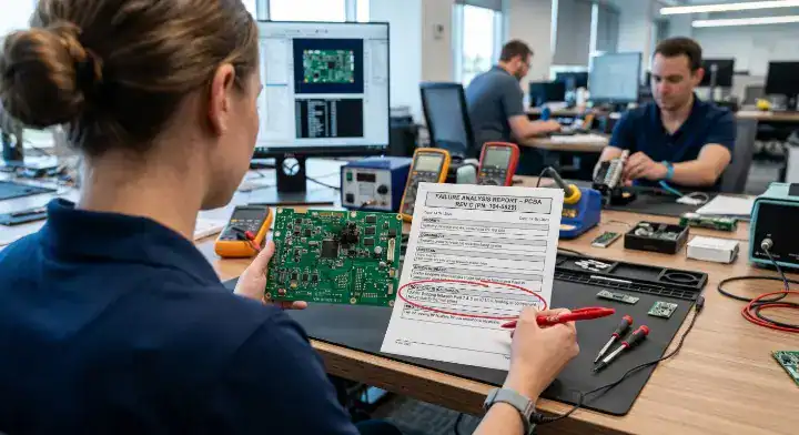
When a board fails in the field, a vague document from your contract manufacturer (CM) leaves you completely vulnerable. You receive an evaluation blaming “operator error” or “component aging,” and your overall field defect rate remains stubbornly unchanged. We fix this imbalance by teaching you exactly how to dissect a pcba failure analysis report like an industry insider. At QueenEMS, we maintain a 99.7% first-pass yield rate because we treat every field return as a strict system upgrade tool, not a meaningless blame-shifting exercise.
1. When Should You Request a Failure Analysis Report From Your CM?
You must request a formal pcba failure analysis report when your field failure rate exceeds 0.5% for commercial products or 0.1% for medical devices. For prototype runs (5–10 boards), request it immediately upon the very first failure to stop bad processes from scaling; for mid-volume production (100–500 boards), trigger an investigation if 3 or more identical failures occur within a single batch.
Look at the math: Waiting for customer complaints to accumulate damages your brand reputation permanently. You need a data-driven trigger point to force your supplier into action.
- Early life failures occurring within the first 90 days of deployment.
- Repeat defects appearing in the exact same board location across different production batches.
- High-value assemblies where a single board replacement costs more than $500.
Bottom line: Never pay for mass production scaling if your prototype field failures lack a documented, 8D-based root cause investigation.
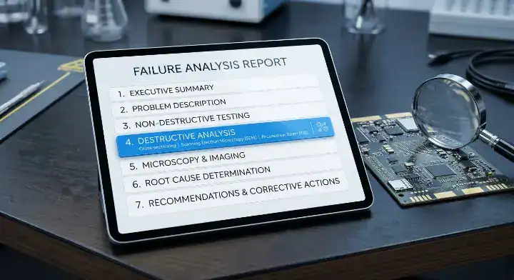
2. What Are the 7 Required Sections of a Complete PCBA Failure Analysis Report?
A compliant pcb failure analysis report contains exactly 7 sections: problem description, sample identification, visual inspection, electrical isolation, destructive analysis, root cause statement, and corrective action plan. Missing any of these 7 sections reduces the document to a mere opinion piece rather than an objective engineering investigation.
According to industry bodies like IPC, a proper report references specific standards. IPC-A-610 defines workmanship acceptance criteria for electronic assemblies. A valid report notes the specific IPC-A-610 section and class (1, 2, or 3) violated, proving the failure is an objective standard violation rather than a CM’s personal judgment call.
| Required Section | What It Should Contain | What You Must Verify | Red Flag if Missing |
|---|---|---|---|
| Problem Description | Exact failure mode from the field | Operating environment details | Vague “board doesn’t work” notes |
| Sample Identification | Serial numbers, date codes, lot numbers | Traceability to specific SMT lines | No batch tracing information |
| Visual Inspection | High-res optical photos of the defect | Visible physical damage or burns | Blurry photos or no images |
| Electrical Isolation | Pinpoint exact failing node/component | I-V curve tracing data | Broad guesses about component areas |
| Destructive Analysis | Cross-section, SEM/EDS, or dye-and-pry | Internal structural proof | Relies entirely on external visuals |
| Root Cause | 5 Whys analysis tracing to process | Links to machine or material | Blames “operator error” directly |
| Corrective Action | Specific parameter or SOP changes | Timeline and implementation owner | “Will train operators more” |
Choose to accept the report if it explicitly maps its findings to IPC standards; choose to reject and return it if it skips the destructive analysis phase entirely.
Bottom line: Treat a report missing the destructive analysis or corrective action sections as an incomplete draft, and force your CM to finish the job.
3. How Do You Tell a Real Root Cause From a Symptom in a FA Report?
A true defect root cause report identifies the specific broken process, with 80% of actual root causes linking back to machine parameters, tooling degradation, or structural training gaps. A symptom is what you physically see (like a cold solder joint), while the root cause is why the system produced it (like a reflow profile thermal soak lasting only 45 seconds instead of the required 90 seconds).
University research on failure analysis methodology emphasizes that field failures must link back to earlier process events to enable true reliability improvement. Without rigorous root cause analysis tying failure mechanisms to specific process steps, reliability prediction tools and corrective actions remain entirely ineffective.
Here is the reality: CMs love to stop at the symptom level to avoid admitting process faults.
- “Solder bridge” is a symptom; a “stencil aperture 15% too large” is the root cause.
- “Defective component” is a symptom; “improper MSL baking destroying the component” is the root cause.
- “Operator error” is a symptom; a “missing poke-yoke fixture allowing backward insertion” is the root cause.
You can learn more about linking symptoms to processes by studying how to prevent cold solder joints in standard manufacturing environments.
Bottom line: If the stated root cause is a person (“operator error”), reject the report and demand the 5 Whys analysis showing exactly why the manufacturing system allowed that person to fail.
4. What Are the Most Common Failure Mechanisms and What Do They Reveal About Your CM?
The three most common failure mechanisms—PTH via opens, electromigration (Pb-dendrite), and thermal fatigue—account for over 60% of field returns and directly expose a CM’s poor process control or cheap material sourcing. For instance, severe PCB delamination points to a 100% failure in material qualification or a total disregard for moisture sensitivity level (MSL) baking protocols.
Last quarter, a customer came to us after 3 of 500 boards from their previous CM failed in the field—all within 8 months of deployment. Their previous CM’s report concluded “failure caused by component aging.” We requested the failed boards. Cross-section analysis revealed all 3 failed boards had IMC (intermetallic compound) layer thicknesses of 6-8 microns at the BGA solder joints, while the normal range is 1-3 microns. This is excessive reflow time consuming too much copper into the solder, creating brittle joints. The customer’s previous CM had not run reflow profile verification in 14 months. We recalibrated the profiles, and the client experienced zero field failures in their next 5,000-unit run.
| Failure Mechanism | Visible Symptom | True Root Cause | CM Management Gap Exposed |
|---|---|---|---|
| PTH Via Opens | Intermittent power loss | Plating thickness too thin | Cheap bare board supplier sourcing |
| Electromigration | Short circuits in humidity | Ionic contamination | Poor wash process / bad flux choice |
| Black Pad (ENIG) | Brittle component drop-off | Nickel corrosion during plating | Poor chemical bath maintenance |
| Thermal Fatigue | Cracked BGA solder joints | Mismatched CTE / bad reflow | Lack of thermal profiling |
| Dewetting | Solder refusing to stick | Heavy oxidation on pads | Storing PCBs outside vacuum bags |
Choose to audit your CM’s sourcing department if you see counterfeit components or bare board plating issues, but choose to audit their SMT process engineers if you see cold solder, excessive IMC growth, or bridging issues.
Bottom line: Use the failure mechanism not just to fix the current board, but to identify exactly which department at your CM needs an immediate operational audit.
5. What Inspection Techniques Should Be Used and What Do They Each Reveal?
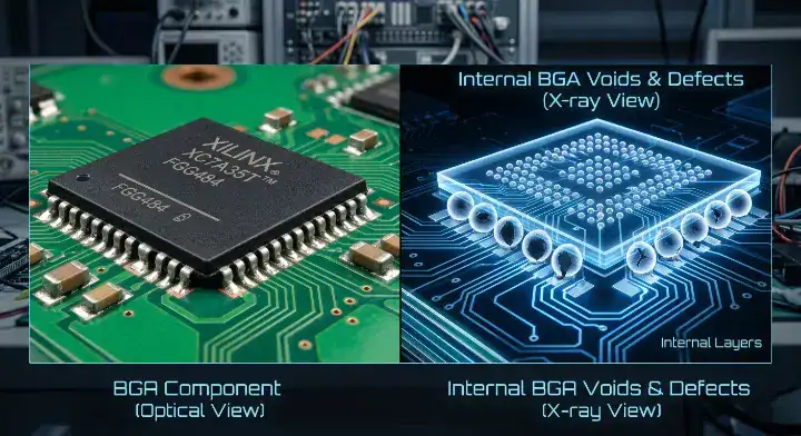
Professional pcba root cause analysis relies on a combination of optical microscopy (detecting 100% of surface anomalies), X-ray imaging (penetrating 100% of hidden BGA joints), and physical cross-sectioning. A basic visual inspection takes 10 minutes and costs nothing, while full SEM/EDS (Scanning Electron Microscopy / Energy Dispersive X-Ray Spectroscopy) analysis requires 2-4 days and costs $300–$800 per sample.
Destructive analysis is a physical testing method that permanently alters or destroys the PCB sample, typically costing $300–$800, to reveal internal structural defects that X-rays cannot see. Similarly, ion chromatography is a chemical analysis method used to measure ionic contamination, requiring a strict limit of less than 1.56 micrograms of NaCl equivalent per square centimeter to pass.
| Inspection Technique | What It Catches | What It Cannot See | Typical Cost |
|---|---|---|---|
| Optical Microscope | Surface cracks, bad fillets | Internal voids, BGA joints | Included / Free |
| 2D / 3D X-Ray | BGA voids, short circuits | IMC layer thickness, micro-cracks | $50 – $150 |
| Cross-Section | Plating thickness, IMC growth | The entire board (destroys sample) | $200 – $400 |
| SEM / EDS | Exact elemental composition | Large macro-structural warpage | $300 – $800 |
| Ion Chromatography | Flux residue, salt contamination | Physical joint strength | $150 – $300 |
Choose X-ray for non-destructive analysis of hidden BGA voids across a large sample size, but choose cross-sectioning and SEM/EDS if you need to measure exact intermetallic compound thicknesses to prove reflow oven failures. You can see how these techniques overlap by comparing AOI vs X-ray vs ICT capabilities.
Bottom line: Never accept a final report for hidden joint failures if the CM only used an optical microscope; demand quantitative X-ray or cross-section data.
6. How Should You Interpret SEM/EDS, X-Ray, and Cross-Section Images?
Interpreting SEM/EDS and cross-section images requires looking for specific measurement deviations, such as an Intermetallic Compound (IMC) layer exceeding 3 microns or X-ray voids occupying more than 25% of a solder ball’s total area. These diagnostic images provide mathematical proof of a failure, removing any subjective arguments or excuses from the supplier.
Pay close attention to this: CMs sometimes include images without measurement scales or annotations, hoping you will just glance at the picture and accept their written conclusion.
- On an X-ray, look for dark circular spots inside the lighter gray solder balls; if those voids exceed 25% of the area, it violates IPC standards.
- On a cross-section, look for the boundary line between the copper pad and the solder; a jagged, overly thick line indicates excessive heat exposure.
- On an EDS graph, look for unexpected elemental peaks; high levels of Chlorine or Bromine indicate severe flux residue contamination.
Bottom line: If your CM provides diagnostic images without specific measurement annotations and acceptable limit ranges, force them to re-issue the document with quantified engineering data.
7. What Corrective Actions Should You Demand After a Failure Analysis?
A permanent corrective action plan must eliminate the physical possibility of the defect recurring, typically reducing specific defect rates by 90% or more within a single production quarter. Promises like “we will train operators” are weak containment actions; true corrective actions involve changing machine parameters, updating software limits, or modifying physical tooling on the factory floor.
A medical device client received a report from us identifying solder paste height variation as the root cause of intermittent BGA failures. Our initial proposal: “increase SPI inspection frequency to 100%.” Their quality engineer pushed back—that was just containment. We re-analyzed and found the stencil had 23 hours of accumulated print time before changeover, exceeding the manufacturer’s 16-hour spec. The true corrective action: implement automatic stencil changeover at 12 hours regardless of visual condition, logging each changeover with a timestamp. That client’s BGA defect rate dropped from 1.2% to 0.08% over the next quarter. A good customer pushes back on weak fixes.
| Action Proposed | Weak Version (Reject) | Strong Version (Accept) | How to Verify Implementation |
|---|---|---|---|
| Operator Error | “Retrain the operator” | “Install physical poke-yoke fixture” | Request photos of the new fixture |
| Solder Voids | “Monitor reflow oven” | “Change Zone 3 soak time to 85s” | Request the new oven profile log |
| Paste Issues | “Clean stencil more” | “Automate cleaning every 10 boards” | Review machine software settings |
| Part Placement | “Add visual check” | “Program AOI to reject >10% shift” | Ask for the updated AOI program file |
Accept a corrective action if it physically changes a machine setting, alters an automated SOP, or introduces a hard physical barrier; reject it immediately if it relies entirely on human memory, increased awareness, or verbal warnings. Reviewing the PCBA rework defects 8 common causes will help you identify what true process fixes look like.
Bottom line: Containment catches the problem today, but only hard, verifiable process changes stop it from bankrupting you tomorrow.
8. What Are the Red Flags in a Failure Analysis Report?
A deceptive failure analysis report uses subjective language and hides behind generic terms, masking the fact that 60-80% of the time, the factory’s own equipment was out of calibration. Phrases like “normal wear and tear” on a 6-month-old board or “NFF (No Fault Found)” without accompanying test logs are immediate indicators that the CM is aggressively avoiding financial liability.
| Red Flag Phrase | What the CM is Actually Hiding | What You Should Ask Instead |
|---|---|---|
| “Component aging” | They bought old, expired parts | “Provide the date codes and MSL logs.” |
| “No Fault Found (NFF)” | They didn’t test it under stress | “Provide thermal cycling test results.” |
| “Operator Error” | The process has no safeguards | “Show me the 5 Whys process analysis.” |
| “Customer design flaw” | They skipped the DFM check | “Why wasn’t this flagged during NPI?” |
If you see “No Fault Found,” push for environmental stress testing to replicate the field environment; if you see “Operator Error,” demand the 5 Whys process analysis. Comparing your CM’s documentation against a standard PCB QC report sample will quickly reveal if they are hiding behind generic templates.
Bottom line: Your CM is a business trying to protect its margins; use these red flags to break through their defensive language and extract the engineering truth.
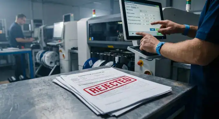
9. How Should You Handle a CM That Refuses to Provide a Proper FA Report?
When a CM refuses to provide a report for field failures, you must escalate the issue to a third-party laboratory, which typically costs $1,500 to $3,500 for an independent, unbiased analysis. To prevent this standoff, your initial procurement contract must dictate who pays for the analysis and state clearly that the CM bears the third-party cost if they are found at fault.
Do not back down: CMs will often claim the boards are “out of warranty” or demand hefty upfront fees to investigate.
- Review your Master Services Agreement (MSA) for specific quality clauses.
- Send the failed units to an independent failure analysis lab without telling the CM.
- Use the independent lab’s findings to force the CM to cover both the replacement boards and the lab fees.
Bottom line: If a CM outright refuses to investigate a field failure, treat it as a massive breach of trust and immediately begin qualifying a secondary supplier.
FAQ
What is a PCBA failure analysis report? It is a formal engineering document detailing the exact root cause of a printed circuit board failure, typically containing 7 sections and utilizing the 8D methodology. It relies on destructive testing and X-ray imaging rather than just visual guesses. Demand this document from your supplier to prevent recurring defects.
When should I request a failure analysis report? Yes, you must request it immediately when your field failure rate exceeds 0.5% for commercial goods or 0.1% for medical devices. Do not wait for complaints to pile up; early life failures within 90 days warrant immediate investigation. Contact your CM the moment you hit these threshold numbers.
Who pays for the PCB failure analysis? The CM typically pays for the analysis if the root cause points to a manufacturing defect, saving you $500–$2,000 in lab fees. However, if the failure stems from your original design flaw, you bear the cost. Always write a clear liability clause in your procurement contract before starting mass production.
What sections are required in the report? Exactly 7 sections are required: problem description, sample identification, visual inspection, electrical isolation, destructive analysis, root cause, and corrective action. If the report lacks destructive analysis (like cross-sectioning) or measurable corrective actions, it is incomplete. Send it back to the quality manager for revision.
What should I do if my CM refuses to investigate a field failure? Immediately hire an independent, third-party laboratory to perform the analysis, which will cost between $1,500 and $3,500. Once the independent lab proves the CM’s manufacturing process caused the failure, use the data to claim financial compensation. Start looking for a more transparent manufacturing partner today.
Reading a vague, defensive analysis document is frustrating and leaves your supply chain exposed to continuous defects. You need a partner who treats every anomaly as an opportunity to harden the production process, not an excuse to hide behind “operator error.”
At QueenEMS, we offer Free DFM/DFA engineering reviews on every order, perform 3D AOI and X-Ray inspection on every single BGA joint, and possess up to 60-layer PCB fabrication capabilities. We provide full turnkey service from component sourcing to final testing. Stop accepting mediocre reports and blame-shifting. Contact us at QueenEMS to build a bulletproof, transparent manufacturing partnership for your next project.
Written by the QueenEMS Engineering Team.
Upload your files today · Free DFM check before production · Ship worldwide
Get your PCB prototypes in as fast as 24 hours. We handle FR4, Rogers, and Flex up to 60 layers — free prototypes for 2–4 layer boards, no minimum order.
Just upload your Gerber + BOM — we source every part, assemble, and inspect (AOI + X‑Ray) so you don't have to chase suppliers. Boards ship in as fast as 24 hours.