
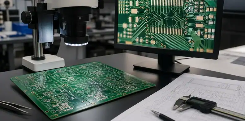
Quick Answer: A high precision PCB RFQ should define the smallest finished line and space, copper weight, layer location, solder mask limits, registration risk, and inspection evidence before suppliers compare price. The buyer should not accept a capability claim unless the quote states whether the target geometry is routine production, engineering review, or a special process exception.
High precision PCB buying becomes risky when the RFQ only says fine line or high accuracy. Those phrases do not tell the fabricator which layer carries the hard feature, whether the copper is thin enough for the target, or what evidence proves the finished board. This page is not a broad tolerance article. It focuses on the manufacturing release questions that decide whether small line-space features can be quoted, inspected, and repeated without hidden CAM assumptions.
Table of Contents
- What does high precision mean in a PCB RFQ?
- Which layer contains the feature that drives cost?
- How should copper weight be connected to line-space?
- Where do mask and registration consume precision margin?
- What evidence should prove the feature?
- How should buyer and supplier handle DFM edits?
- How should quotations be compared?
- What should QueenEMS receive for line-space review?
- How should buyers lock the precision baseline?
What does high precision mean in a PCB RFQ?
High precision should mean named finished features, not a general quality label. The RFQ should identify the minimum trace width, minimum spacing, copper weight, layer number, finished thickness, solder mask condition, and whether the geometry is isolated or repeated across the board.
The broader PCB fabrication tolerances article explains which tolerances deserve cost. This article starts after that decision, when the buyer needs suppliers to quote the actual fine-feature manufacturing risk.
Definition rule: high precision is quotable only when the controlled geometry and layer location are visible.
Which layer contains the feature that drives cost?
The cost driver may sit on one inner layer, one outer BGA escape area, a flex tail, or a dense connector region. A supplier cannot judge the job from the smallest number alone because density, copper thickness, and local copper balance change process difficulty.
Ask the supplier to mark the limiting feature in CAM review. That turns the RFQ into a real production question: which layer and region forces slower etching, tighter imaging, extra inspection, or lower panel utilization?
CAM signal: require a marked limiting feature instead of accepting a general fine-line capability statement.
| RFQ item | What to mark | Why it changes the quote |
|---|---|---|
| Critical layer | Layer number and local feature area | Prevents the whole stack-up from being priced as the tightest layer |
| Finished copper | Required copper after processing | Connects line-space feasibility to etch margin |
| Evidence request | Coupon, photo, or measurement report | Makes acceptance review part of the quoted scope |

How should copper weight be connected to line-space?
Copper thickness and line-space cannot be reviewed separately. Thicker copper can make etching compensation harder, reduce spacing margin, and increase the chance that a nominal design target does not match the finished feature.
If the same design also has heavy copper areas, connect the quote to PCB copper balance review. A dense fine-line region beside large copper pours can become a different process problem than a simple fine-line coupon.
Copper call: quote the minimum feature together with copper thickness and local copper density.
Where do mask and registration consume precision margin?
A fine copper feature can still fail the product if solder mask registration, legend clearance, or layer-to-layer registration consumes the remaining margin. Dense pads, small dams, and exposed copper near fine spacing need a mask review before release.
Use solder mask opening requirements for the mask details. In this RFQ, ask whether the mask and registration assumptions protect the same features that make the PCB high precision.
Registration rule: do not approve fine copper geometry while leaving mask and layer alignment as generic notes.
What evidence should prove the feature?
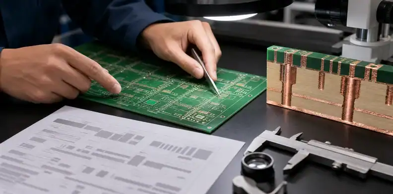
Evidence should prove the limiting feature, not a convenient wide trace. Ask whether the supplier will use AOI records, dimensional measurement, coupon data, microsection evidence, or first-article photos for the specific fine-feature region.
For hidden layer or hole-related proof, PCB microsection evidence may be more useful than a surface photo. The evidence choice should match the feature that can stop acceptance.
Proof rule: inspection points should represent the hardest geometry in the released design.
| Evidence type | Best use | Buyer acceptance note |
|---|---|---|
| CAM screenshot | Confirms the supplier found the narrow area | Useful before tooling release |
| Microsection or coupon | Supports finished copper and spacing evidence | Better for first-article or production approval |
| Outgoing inspection note | Documents lot-level release | Should name the same controlled feature as the drawing |
How should buyer and supplier handle DFM edits?
DFM edits may include line widening, spacing relaxation, teardrops, pad changes, solder mask relief, or local copper adjustments. Some edits preserve the product; others change impedance, current, fit, or component compatibility.
A clean RFQ says which features are design-critical and which may be proposed for manufacturing. The supplier should return marked edits before CAM approval, not after tooling has already started.
Approval boundary: any change to the limiting high-precision feature needs named engineering approval.

How should quotations be compared?
Compare high precision quotes by assumptions: routine capability, special review, extra inspection, modified artwork, minimum order quantity, and yield risk. A lower unit price may simply omit the evidence or assume relaxed geometry.
Procurement should ask each supplier to state the same finished line-space target, copper condition, inspection plan, and allowed DFM changes. Only then does price comparison describe the same board.
Price rule: a cheaper quote is not comparable if it silently changes the fine-feature acceptance basis.
What should QueenEMS receive for line-space review?
QueenEMS should receive Gerber or ODB++ files, stackup, copper weights, controlled feature callouts, solder mask layer, target quantity, and any supplier CAM comments. Send the package through the QueenEMS contact page so the response can separate routine fabrication, engineering-review features, DFM approval items, and evidence needed before order release.
The best review happens before suppliers quote from incomplete language. Once one supplier assumes relaxed spacing and another assumes special inspection, the buyer no longer has a clean comparison.
RFQ close: make the limiting geometry measurable, locatable, and owned before price is negotiated.
How should buyers lock the precision baseline?
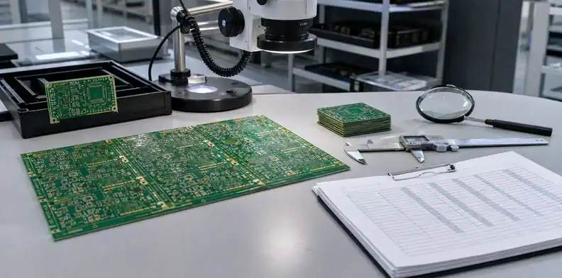
A high precision PCB baseline should be a short record that purchasing can reuse, not a private CAM assumption. Keep the accepted minimum line and space, copper weight, layer location, solder mask decision, measurement method, and supplier DFM response together with the released revision. That record tells the next buyer what was actually approved, not only what the CAD file nominally shows.
A useful RFQ sentence is: “Quote the released high precision PCB data with minimum finished line and space controlled on the marked layers. Supplier must identify the limiting feature, copper thickness assumption, measurement method, and any proposed CAM change before production release.” This wording gives the supplier a concrete answer path without forcing them to reveal process details that do not help the buyer.
The supplier response should not be accepted if it only says “can make it.” A stronger answer identifies whether the feature is standard production, engineering review, or a special process condition. It also names the inspection evidence that will be available at shipment. If the answer changes line width, solder mask clearance, or local copper, the buyer should see a marked screenshot before approval.
For dense BGA or connector regions, compare the high-precision feature against assembly risk. A trace that is manufacturable may still leave solder mask dams too narrow, pads too exposed, or rework margin too small. The fabrication RFQ should therefore be reviewed with the assembly drawing when the fine feature sits under a component interface.
Controlled impedance can also change the decision. A supplier may propose a trace-width adjustment to improve etching yield, but that adjustment may change impedance if the feature belongs to a controlled pair. The quote package should identify which fine traces are electrically controlled and which are only routing-clearance features.
For first lots, ask for evidence that represents the hard feature. A measurement on an easy outer trace does not prove a dense inner feature. If the supplier uses a coupon, ask how the coupon relates to the real layer and copper condition. If the supplier measures the board, ask which location will be measured and whether that location is representative.
The buyer should also decide what happens when the measurement is marginal. Some jobs can accept a supplier deviation after engineering review; others should stop before shipment. That decision should not be improvised by receiving inspection. Define whether a marginal feature requires rework, concession, reorder, or engineering disposition.
Second sourcing needs extra care. Another factory may meet the same nominal line and space with a different compensation method, inspection plan, or yield assumption. Give the second source the accepted baseline and ask them to state differences before price comparison. Otherwise the buyer may approve a cheaper quote that does not build the same controlled geometry.
The final record can be simple: revision, limiting layer, minimum feature, copper weight, mask rule, evidence, supplier edits, and approval owner. It gives purchasing a way to quote repeat production without turning every reorder into a new fine-line negotiation.
For cost-down reviews, separate process margin from product margin. A buyer may ask whether the line-space target can be relaxed, but the answer should come from electrical, mechanical, and assembly owners rather than from price pressure alone. If the tight feature only exists because an earlier layout used conservative escape routing, a controlled redesign may be possible. If the feature protects impedance, creepage, connector escape, or package fit, relaxing it can move the risk into the product.
A practical supplier-comparison table can include five rows: limiting feature, copper thickness, supplier process status, inspection evidence, and allowed DFM edits. The table does not need proprietary process windows. It only needs enough information to show whether Supplier A and Supplier B are quoting the same finished geometry.
High precision also changes schedule risk. A supplier may accept the job but require engineering review after CAM, which can move the real approval date later than the purchase order date. Ask whether the quote is ready for immediate CAM release or whether it depends on a post-order feasibility check. That answer helps purchasing avoid a false lead time.
If the first lot uses an engineering deviation, record whether the deviation is temporary or becomes the new baseline. Prototype concessions are often reasonable, but they should not silently become production approval. Mark the order as engineering validation when the feature is still being tuned.
For PCB incoming inspection, the buyer should not try to measure every fine trace without the right equipment. Instead, file the supplier evidence, inspect obvious workmanship, and compare any critical photos or report values against the release record. If the customer requires independent measurement, define that before quotation so the supplier knows the evidence chain.
The final high precision PCB package should answer four questions: what is the hard feature, where is it located, how will it be proven, and who approves any change. If those questions are closed, the supplier can quote a manufacturable board instead of guessing what precision means.
For schedule planning, ask whether the supplier needs an engineering query before tooling. A line-space target that is feasible after small CAM changes is different from a target that requires customer redesign. Put that answer in the quote comparison so the buyer sees technical delay before the PO is placed.
If the supplier asks to relax geometry, require them to identify the exact affected nets or features. A blanket relaxation request may hide one tight corner, one BGA escape, or one local mask problem. Engineering can often approve a targeted change faster than a broad redesign request.
For production release, store the supplier’s final CAM assumption with the order. If the first lot passes because the supplier used a specific compensation method, future lots should not restart from the raw Gerbers without that note. High precision work stays stable when the accepted manufacturing interpretation is part of the product file.
A final quote-readiness check should also include what the buyer will not pay for. If the product does not need a fine-feature area on every layer, say which layers are ordinary. That can prevent a supplier from pricing the whole board as if every layer carries the same narrow process margin.
The buyer should ask whether the feature is controlled by finished copper, artwork width, or assembly clearance. Those are different acceptance points. Finished copper belongs to fabrication evidence; artwork width belongs to CAM change control; assembly clearance may belong to solder mask or component fit.
For high precision PCB sourcing, the cleanest handoff is a marked PDF plus native manufacturing data. The PDF shows the supplier what matters; the native data lets CAM inspect it. Sending only one of those files invites either technical ambiguity or manual interpretation.
If the buyer is close to release, one more practical step is to ask for the supplier’s exception list in writing. The list should say whether the high precision PCB can be built as released, whether the supplier needs local compensation, and whether any measurement or evidence is excluded from the base quote. This protects the buyer from approving a price that later depends on unpriced engineering review.
For production lots, the buyer should define whether every lot needs the same evidence or whether first-lot evidence is enough. High precision features that are customer-critical may need recurring proof; lower-risk features may only need first-article confirmation and normal outgoing inspection. That decision affects cost and lead time, so it belongs in the RFQ rather than in a shipment dispute.
For repeat orders, the buyer should keep the high-precision note tied to the revision, not only to the purchase order. A future buyer may reuse the old order text without realizing that the fine feature was approved under a different copper weight, solder mask opening, or stack-up. Revision-controlled notes make the next quote review faster and reduce the chance that a supplier treats an old exception as a standing approval.
The safest comparison is not the lowest line item price; it is the quote that states what has been included in the fine-line review. A supplier that names the narrow trace layer, finished copper assumption, imaging compensation, and inspection evidence gives the buyer a cleaner basis for approval than a supplier that simply says the board is “OK to build.” That distinction matters when the design is close to a process limit.
FAQ
Is high precision PCB the same as HDI?
No. HDI usually refers to density and microvia architecture; high precision can also mean fine line-space, tight registration, or controlled fabrication limits on a non-HDI board. The RFQ should name the exact feature that creates the precision requirement.
Should I ask every supplier for their smallest line width?
No. Ask for routine production capability at your copper weight and layer type, then ask what evidence proves the finished feature. A best-case demo number is less useful than a quoted feature tied to your actual stackup and panel.
Can CAM change fine traces to improve yield?
Only after engineering approves the affected features and the supplier marks what changed. Fine-feature edits can affect impedance, clearance, current capacity, solder mask, or assembly escape routing.
Sources
- IPC, IPC-2221C Generic Standard on Printed Board Design
- IPC, IPC-6012 Qualification and Performance Specification for Rigid Printed Boards
Written by the QueenEMS Engineering Team
Upload your files today · Free DFM check before production · Ship worldwide
Get your PCB prototypes in as fast as 24 hours. We handle FR4, Rogers, and hybrid boards up to 40 layers in volume production, with advanced builds subject to engineering review — free prototypes for 2–4 layer FR-4 boards, no minimum order.
Just upload your Gerber + BOM — we source every part, assemble, and inspect (AOI + X‑Ray) so you don't have to chase suppliers. Boards ship in as fast as 24 hours.