
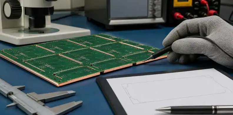
Quick Answer: PCB edge plating acceptance is a finished-board decision: does the supplied edge match the approved drawing, connect where required, remain clear where prohibited, and meet the agreed visual and electrical checks? Compare a marked edge map with the actual board, inspect exposed plated edges for discontinuity or damage, review the lot-linked test evidence, then release, hold, or document an approved deviation.
PCB edge plating can serve grounding, shielding, mechanical contact, or package-interface functions. The mistake is to treat it like a decorative perimeter finish when the real risk is copper-to-edge geometry, routing sequence, and continuity evidence. The edge-plating requirements guide covers how to specify the feature before fabrication. This page focuses on inspecting and accepting the finished plated edge and its release records.
Table of Contents
- What must edge plating acceptance define?
- Which edges should be plated and which must stay clear?
- How does routing sequence affect plated edge quality?
- What evidence proves continuity or shielding?
- Where do RF and shielding requirements change the review?
- How should CAM changes be approved?
- How should suppliers be compared?
- What should QueenEMS receive for edge-plating review?
- How to inspect and release a plated edge
What must edge plating acceptance define?
Acceptance must define the plated edge, purpose, connected copper, keepout areas, thickness or continuity evidence, and visual limits. A board can have partial edge plating, full perimeter plating, castellated areas, or shield-connected edges, and each case needs a different acceptance rule.
The existing PCB edge plating requirements page owns the general requirement. This page asks what proof and supplier response make the quote safe to release.
Acceptance rule: edge plating should be tied to a function, not only to a drawing color.
Which edges should be plated and which must stay clear?
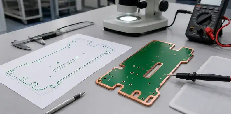
The drawing should mark plated edges separately from non-plated routed edges. It should also show keepouts where copper must not wrap, where solder mask must protect a region, or where enclosure clearance limits exposed metal.
Use PCB copper-to-edge clearance when the same board has sensitive spacing near the outline. Edge plating can intentionally violate ordinary copper pullback, so the drawing must say where that is allowed.
Boundary call: plated-edge regions and copper-clearance regions must not be left for CAM to infer.
| Drawing area | Control needed | RFQ note |
|---|---|---|
| Outer board edge | Plated length and finish boundary | Mark the exact side or segment |
| Routed slot | Plating continuity around the slot wall | Confirm whether the slot is functional |
| Chassis contact edge | Net identity and contact surface | Name the grounding or shield requirement |
How does routing sequence affect plated edge quality?
Routing sequence affects whether the edge can be plated cleanly and then finished without tearing copper, leaving burrs, or exposing unwanted laminate. The supplier may need a special process sequence, tabs, or panel support to protect the plated edge.
This also connects to PCB board outline tolerance because edge geometry and plating condition meet at the final route.
Process signal: ask how the supplier will preserve the plated edge during final routing and handling.
What evidence proves continuity or shielding?
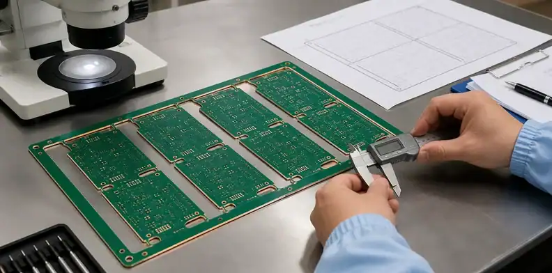
Evidence may include continuity testing, visual inspection, thickness reporting, marked photos, or microsection where the plated edge ties into internal copper. The correct evidence depends on whether the edge is a shield, ground return, contact surface, or mechanical feature.
For buried evidence, PCB microsection report requirements can help define whether a cross-section or representative coupon is worth requesting.
Proof rule: edge-plating evidence should prove the electrical or mechanical function that justified the process.
Where do RF and shielding requirements change the review?
RF and shielding boards need a stricter review because edge plating can affect return paths, enclosure contact, antenna isolation, and EMI behavior. The supplier should know whether the plated edge is a grounding convenience or a controlled RF feature.
For projects with RF packaging or shield contact, connect the quote to QueenEMS RF PCB manufacturer capability so the plated edge is reviewed with the stackup and launch region.
RF call: do not let the supplier treat a controlled shield edge as a cosmetic metal finish.
| Evidence | What it confirms | When to require it |
|---|---|---|
| Continuity check | Electrical connection to the intended net | Functional shield or grounding edge |
| Edge photo | Workmanship after routing | First article and customer-critical surfaces |
| Sampling record | Lot release basis | Repeat production with stable panelization |
How should CAM changes be approved?
CAM changes may include edge pullback adjustment, tab relocation, solder mask relief, route compensation, copper tie modification, or plated-edge length changes. Some changes are harmless; others break the grounding or enclosure interface.
Ask the supplier to return a marked edge-plating view before CAM release. The buyer should approve the plated boundary, non-plated sections, and any support-tab evidence that affects final appearance.
CAM boundary: approve edge-plating geometry visually before production tooling begins.

How should suppliers be compared?
Compare suppliers by plated-edge process assumptions, evidence, continuity testing, routing approach, lead time, and cosmetic criteria. One quote may omit continuity evidence; another may include it and therefore look higher.
The buyer should also ask whether the supplier treats edge plating as routine or engineering review. That answer can matter more than the unit price when the feature controls shielding or contact reliability.
Quote rule: compare the plated-edge evidence package before choosing on price.
What should QueenEMS receive for edge-plating review?
QueenEMS should receive fabrication data, plated-edge drawing, copper-to-edge notes, stackup, shield or ground purpose, enclosure contact requirement, quantity, and desired evidence. Send it through the QueenEMS contact page so the response can identify unclear edge boundaries, clearance conflicts, evidence needs, and supplier assumptions before RFQ release.
A clean package lets the supplier quote plated edge processing as a controlled feature instead of discovering the requirement after CAM starts.
RFQ close: define edge plating as a functional acceptance item when it affects shielding, contact, or grounding.
How to inspect and release a plated edge
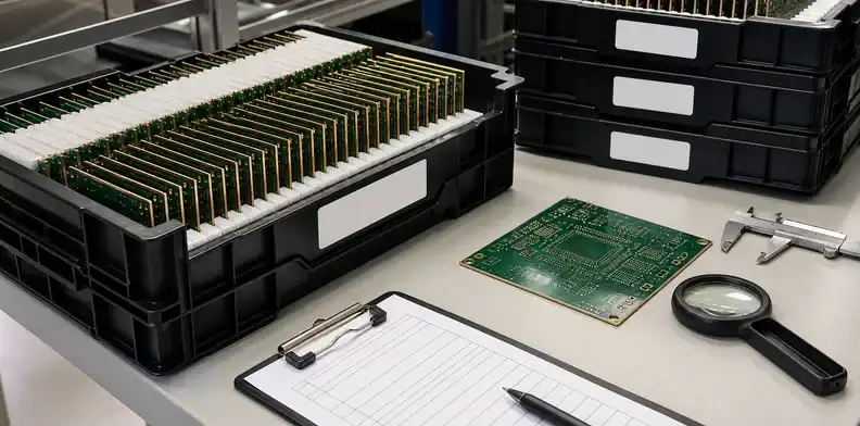
Use the approved fabrication drawing and CAM disposition as the reference. First identify every plated segment and every intentional gap or non-plated edge. Inspect the actual routed edge under appropriate magnification for missing coverage, obvious damage, burrs, mask encroachment, or metal where a clearance was required. A photograph alone does not establish electrical continuity.
| Acceptance check | Evidence to request | If it fails |
|---|---|---|
| Plated boundary | Marked drawing plus finished-edge photos or inspection record | Hold boards with missing plating or metal in a keepout |
| Electrical function | Continuity/isolation test points and lot-linked results, when the edge is functional | Hold and confirm the approved test setup; do not infer continuity from appearance |
| Workmanship and finish | Inspection criterion agreed in the drawing/order; representative sample and lot ID | Record the location, quantity and defect; seek engineering disposition |
| Revision and shipment | Part/revision/lot traceability, approved CAM change, packing protection | Do not release an unapproved geometry or substitution |
Illustrative decision: if a shield-connected edge has continuous visible plating but the agreed continuity test fails, the lot is on hold. If the edge is electrically acceptable but a non-plated clearance has been bridged, the lot is also on hold. The customer or design authority—not the photograph or this article—sets the final acceptance threshold and approves any deviation.
If the feature is only decorative or for handling, electrical test may be unnecessary; state that explicitly in the purchase specification. For an RF shield or contact edge, define the actual connection and isolation points before production, and retain the measured results with the shipped lot. Keep this inspection record separate from the broader edge-plating design requirements.
A repeat order should reuse the same controlled edge map and acceptance method unless the drawing revision changes. If the supplier proposes a route, finish, or edge-geometry change, obtain design approval before treating the next lot as equivalent.
FAQ
Is PCB edge plating the same as castellated holes?
No. Castellated holes are plated half holes along an edge, while edge plating may cover an edge or perimeter for shielding, grounding, or contact. A board can have one, both, or neither.
Does every plated edge need continuity testing?
Ask for it when the edge is part of a ground, shield, or contact path. Cosmetic edge plating may need visual evidence instead, but the RFQ should say which rule applies.
Can edge plating reduce copper-to-edge clearance?
Yes, intentionally in the plated region, but the drawing must show where exposed edge copper is allowed. Non-plated edges still need their own clearance rule.
Sources
- IPC, IPC-2221C Generic Standard on Printed Board Design
- IPC, IPC-6012 Qualification and Performance Specification for Rigid Printed Boards
Written by the QueenEMS Engineering Team
Upload your files today · Free DFM check before production · Ship worldwide
Get your PCB prototypes in as fast as 24 hours. We handle FR4, Rogers, and hybrid boards up to 40 layers in volume production, with advanced builds subject to engineering review — free prototypes for 2–4 layer FR-4 boards, no minimum order.
Just upload your Gerber + BOM — we source every part, assemble, and inspect (AOI + X‑Ray) so you don't have to chase suppliers. Boards ship in as fast as 24 hours.