
Blog
PCB fabrication, PCB assembly, PCB materials, DFM, SMT, HDI, ceramic PCB, and electronics manufacturing guides from QueenEMS.
IPC-2226 HDI Types: How to Choose Type I, II, or III
Quick Answer: How to Choose Your HDI Type — Type I has one microvia layer on one or both sides of a…
How to Match HDI PCB Materials to Your Application’s Signal Speed
Table of Contents 1. What Is HDI PCB Material Selection and Why Does It Matter for Signal Integrity? 2. How Do You…
How to Verify HDI Microvia Thermal Test Results
HDI microvia thermal cycling needs representative coupons and defined test conditions. Check resistance references, reflow profiles and report limits….
How to Compare HDI Sequential Lamination Costs
HDI sequential lamination cost depends on construction and quote scope. Compare buildup operations, panel charges, setup and redesign trade-offs….
How to Calculate HDI Microvia Aspect Ratio
HDI microvia aspect ratio needs defined depth, diameter and tolerances. Check the calculation, fabrication limits and what geometry cannot prove….
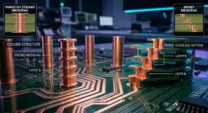
How to Choose Stacked vs Staggered Microvia Layouts
Quick Answer: Stacked microvias place successive connections above one another; staggered microvias offset those connections laterally. Stacking can solve a congested BGA…
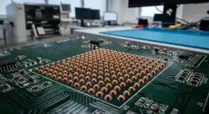
How to Choose Between Copper Fill vs Resin Fill for Via in Pad Design
Table of Contents Every week, a designer asks us why their high-density BGA board failed X-ray inspection. They thought specifying “plugged vias”…
Ceramic PCB Thermal Cycling: How to Test for Failure
Design ceramic PCBs for -40 to 150 C cycling with better substrate choice, metallization and layout decisions for power and automotive reliability….
How to Prevent Ceramic PCB Warping After Eutectic Bonding
Prevent ceramic PCB warping after eutectic bonding by controlling copper symmetry, fixture limits, flatness, ramp rate and die-attach stress….
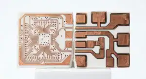
DBC and DPC Ceramic PCB: How to Choose the Right One
DPC or DBC for your ceramic PCB? Compare line width, current handling, thermal path and cost side by side, with a decision table for power and RF designs….
HTCC vs LTCC Ceramic PCB: Compare Before You Choose
HTCC or LTCC for your co-fired ceramic design? Compare firing temperature, conductor metals, cost and RF fit for power, RF and hermetic packages….
How to Choose Thick Film vs Thin Film Ceramic PCB
Compare thick film vs thin film ceramic PCB by deposited materials, patterning, conductor geometry and test evidence. Check when DPC is a separate alternative….