
Quick Answer: HDI sequential lamination costs add exactly $17 to $29 per manufacturing panel per cycle in combined material, labor, and yield loss. While standard PCBs require just one lamination cycle, an HDI Type II (2+N+2) requires three cycles, pushing your total fabrication cost to roughly 3.5× the base standard PCB price. Key takeaways:
- Each lamination cycle adds $17 to $29 per panel in direct manufacturing expenses.
- HDI Type I (1+N+1) costs roughly 2.5× a standard PCB, while ELIC designs reach 5–7×.
- Redesigning a 3-level stacked microvia to use buried vias can save 15–25% by eliminating one risky press cycle.
- Accepting a 5–10% larger board outline can eliminate an entire lamination cycle, saving up to 30% on volume runs.
You design a dense high-speed board, optimize your routing, and submit it for quoting, only to suffer sticker shock when the price comes back at 400% of your standard runs. The culprit is not the copper weight or the surface finish; it is the hidden multiplier of HDI sequential lamination cycles. Understanding the true HDI sequential lamination cost structure enables you to restructure your layer pairs, eliminate unnecessary press cycles, and reduce your overall fabrication budget by up to 40%.
Table of Contents
- #1 What Is HDI Sequential Lamination and Why Does It Cost So Much?
- #2 How Many Lamination Cycles Does Your HDI Design Actually Need?
- #3 What Is the Real Cost Adder Per Lamination Cycle?
- #4 How Does HDI Type (I / II / III) Affect Total Lamination Cost?
- #5 Can You Redesign to Reduce Lamination Cycles?
- #6 When Is Sequential Lamination Cheaper Than Stacked Microvias?
- #7 What Drives the Per-Cycle Cost Beyond Material?
- #8 How Should You Budget for HDI Sequential Lamination?
- #9 How Do You Get an Accurate HDI Cost Estimate Up Front?
1. What Is HDI Sequential Lamination and Why Does It Cost So Much?
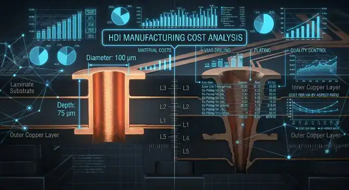
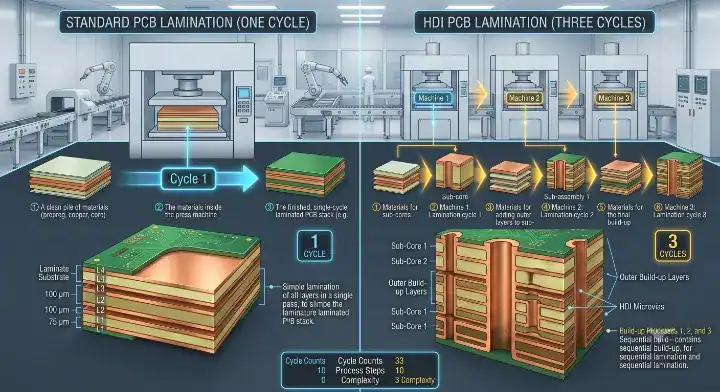
HDI sequential lamination is a fabrication process where layer pairs are pressed, laser-drilled, and plated multiple times, multiplying your base cost by 2.5× to 7×. Every additional lamination cycle adds $17–$29 per panel because it forces the factory to repeat the entire core manufacturing loop from scratch.
Sequential lamination is the repetitive pressing of copper foil and prepreg over an existing cured core. It contrasts with standard PCB manufacturing, where all layers are stacked and pressed exactly once. Because microvias are blind and tiny, lasers cannot drill through the entire board at once; the board must be built up layer by layer, driving up the HDI sequential lamination cost exponentially.
Here is the hard truth:
- The core layer pair is laminated under extreme heat and pressure.
- Microvias are laser-drilled into the newly added dielectric material.
- The vias are plated with copper to establish an electrical connection.
- Outer layers are added, and the board goes back into the press for another cycle.
Bottom line: Every sequential lamination cycle repeats the entire fabrication loop, compounding your machine time and labor costs exponentially.
2. How Many Lamination Cycles Does Your HDI Design Actually Need?
Your HDI design needs one base lamination cycle plus one additional cycle for every level of stacked microvias you include. A standard 1+N+1 stackup requires 2 total cycles, while a complex 3+N+3 stackup requires 4 total lamination cycles to complete the build.
To calculate your cycles, you simply look at the cross-section of your blind vias. If you require a microvia that spans from layer 1 to layer 2, that is a 1-level structure requiring a second press cycle. If your HDI PCB manufacturing services partner needs to stack a layer 1-to-2 via on top of a layer 2-to-3 via, that 2-level structure demands a third press cycle.
Think about it this way:
- Standard multi-layer boards require 1 total cycle.
- A 1-level microvia (1+N+1) requires 2 total cycles.
- A 2-level stacked microvia (2+N+2) requires 3 total cycles.
| HDI Stackup Type | Microvia Levels | Total Lamination Cycles | Relative Manufacturing Time |
|---|---|---|---|
| Standard PCB | 0 | 1 | Base Time |
| 1+N+1 | 1 | 2 | + 1 to 2 Days |
| 2+N+2 | 2 | 3 | + 3 to 4 Days |
| 3+N+3 | 3 | 4 | + 5 to 6 Days |
| ELIC | Every Layer | 5 to 7 | + 7 to 10 Days |
| If your design can route successfully on a 1+N+1 stackup, choose it over a 2+N+2 to instantly shave 3-4 days off your lead time and save one full lamination cycle. |
Bottom line: Your maximum stacked microvia depth directly dictates your minimum required lamination cycles.
3. What Is the Real Cost Adder Per Lamination Cycle?
Every sequential lamination cycle adds exactly $17 to $29 per manufacturing panel to your total cost. For a typical 200-unit production run, a 1+N+1 build costs $15–$25 more per unit than a standard PCB, while a 2+N+2 build adds $35–$50 per unit.
A frequent complaint on the EEVBlog Forum is: “Why is my HDI quote 3-5x the cost of standard PCB? My fab says ‘sequential lamination cycles’ but refuses to break the cost down.” We believe in complete transparency regarding your HDI sequential lamination cost.
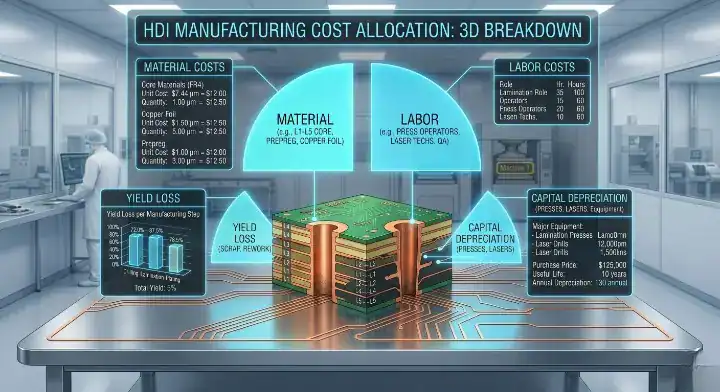
On our HDI line, we track per-cycle cost in four buckets: material, labor, yield, and equipment depreciation. A typical sequential lamination cycle adds about $4-6 in prepreg and copper foil, $8-12 in labor for press setup and post-laminate inspection, $2-5 in yield loss (each cycle compounds the failure probability), and $3-6 in capital depreciation on our lamination presses, which are seven-figure assets. That works out to $17-29 per cycle per panel. On a typical 24-up panel, divide by utilization to get unit cost. We share this HDI vs standard PCB cost comparison openly during quoting because most overpay for HDI when they don’t realize a stackup choice that adds one extra cycle costs them an extra $0.70-$1.20 per unit at production volume.
Let’s break down the math:
- Material Adder: Extra prepreg and copper foil ($4-6/panel).
- Labor Adder: Setup, handling, and inspection time ($8-12/panel).
- Yield Adder: Cumulative failure probability loss ($2-5/panel).
- Capital Depreciation: $1M press amortization ($3-6/panel).
| Cost Category | Expense Per Panel | Impact on Production Run (500 units) |
|---|---|---|
| Material (Prepreg/Copper) | $4 – $6 | Low |
| Labor (Setup/Inspection) | $8 – $12 | High |
| Cumulative Yield Loss | $2 – $5 | Medium to High |
| Capital Equipment Depreciation | $3 – $6 | Medium |
| Total Per Cycle Adder | $17 – $29 | Significant |
| If you are prototyping 10 boards, choose to focus on setup labor which dominates unit cost; if you are running 1,000 boards, choose to optimize for cumulative yield loss. |
Bottom line: You are paying primarily for machine time, physical handling labor, and cumulative yield loss, not just extra fiberglass and copper.
4. How Does HDI Type (I / II / III) Affect Total Lamination Cost?
Moving from a standard PCB to an HDI Type I (1+N+1) multiplies your base cost by 2.5×, while a Type II (2+N+2) hits 3.5×, and ELIC reaches 5–7×. The IPC-2226A HDI design standard defines these structures: Type I requires one sub-lamination, Type II requires two, and Type III needs three or more.
Designers on Reddit frequently ask: “What is the cost difference between 1+N+1 vs 2+N+2 vs ELIC stackups? Looking for hard cost multipliers.” The absolute dollar amount depends on your layer count, but the multiplier remains relatively stable. In prototype stages (<50 pcs), the multiplier skews higher because setup costs are not diluted. In production (500+ pcs), multipliers settle toward the lower bounds. ELIC (every-layer-interconnect) remains the most expensive configuration, reserved almost exclusively for smartphones and dense AI processors.
Why do these multipliers jump so drastically?
- Type I uses a single microvia layer pair, keeping failure points low.
- Type II stacks microvias across two dielectric layers, compounding alignment errors.
- Type III introduces complex staggered structures requiring 4 or more press sessions.
- Comparing these is the foundation of choosing HDI stackup configurations 1+N+1 vs 2+N+2 vs ELIC.
| IPC-2226 HDI Type | Common Configuration | Lamination Cycles | Expected Cost Multiplier |
|---|---|---|---|
| Standard PCB | Multi-layer through-hole | 1 | 1.0× (Base) |
| Type I | 1+N+1 | 2 | 2.5× |
| Type II | 2+N+2 | 3 | 3.5× |
| Type III | 3+N+3 | 4 | 4.5× to 5.0× |
| ELIC | Every Layer Interconnect | 5+ | 5.0× to 7.0× |
| If your component pitch is 0.5mm or larger, choose Type I (1+N+1) to keep costs near 2.5×; if you are routing a 0.35mm pitch BGA, you must budget for a 3.5× to 5.0× multiplier. |
Bottom line: Every time you step up an IPC HDI Type category, expect your fabrication cost multiplier to increase by a full 1.0×.
5. Can You Redesign to Reduce Lamination Cycles?
Yes, you can reduce your HDI sequential lamination cost by 20–30% simply by redesigning your via structures and layer pairs to eliminate one full cycle. A 5-10% increase in board area can often provide enough routing breakout space to drop from a 2+N+2 stackup down to a 1+N+1 stackup.
Engineers on Sierra Connect often ask: “Can I reduce sequential lamination cycles by changing my stackup? Where are the real savings?” The answer is that your designer and your fabricator must work together. While a layout engineer controls the microvia density, the factory controls how those vias translate into physical press cycles.
A drone manufacturer in Arizona sent us a 10-layer HDI design with a 2+N+2 stackup, three buried via layer pairs, and 2-level stacked microvias across the entire BGA region. Total lamination cycles: 5. Our initial quote came in at $48/unit at 500 pcs. The customer pushed back on cost. We sat down with their layout engineer for 90 minutes and identified two changes: (1) consolidate two of the functional groups onto adjacent layer pairs, eliminating one buried via cycle, and (2) reduce stacked microvia depth from 2-level to 1-level by accepting a 6% larger board outline. Revised lamination cycles: 3. New quote: $31/unit. Total project savings on 500 units: $8,500. Same electrical function, same form factor compatibility, same reliability.
Here is the secret to reducing cycles:
- Consolidate functional circuit groups onto adjacent layer pairs.
- Replace deep stacked microvias with buried vias where routing space allows.
- Accept a slightly larger board outline to gain perimeter breakout channels.
- Reduce unnecessary microvia density outside the critical BGA regions.
| Cost Reduction Strategy | Expected Cost Savings | Implementation Difficulty |
|---|---|---|
| Consolidate functional groups to single layer pair | 15% – 20% | Medium |
| Accept 5-10% larger board outline for fewer cycles | 20% – 30% | Low |
| Substitute 3-level stacked vias with buried vias | 10% – 15% | High |
| Remove microvias outside main BGA footprint | 5% – 10% | Low |
| If you are in the schematic phase, choose to consolidate functional groups for a high ROI on cost savings; if your layout is already 80% finished, choose to selectively remove perimeter microvias for an easier fix. |
Bottom line: Your PCB designer controls your lamination cycles; engage your fabrication engineer during the schematic phase, not after layout.
6. When Is Sequential Lamination Cheaper Than Stacked Microvias?
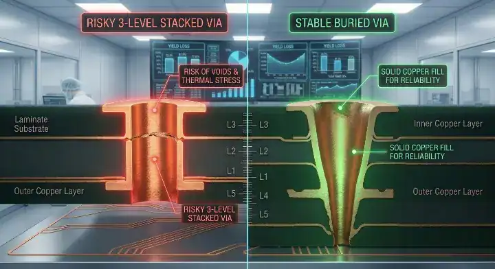
Sequential lamination using buried vias is 15–25% cheaper than using 3-level stacked microvias because it entirely avoids the catastrophic yield drops associated with triple-stacked plating. However, for a 2-level depth, both methods require exactly 3 lamination cycles, making their costs virtually identical.
A common query on Electronics Stack Exchange asks: “Is buried via cheaper than stacked microvia in terms of lamination cost? My design tool offers both.” Buried vias require one extra sub-lamination (you laminate the pair, drill it, then add outer layers). Stacked microvias require n+1 laminations. A 2-level stacked microvia needs 3 laminations, and one buried via layer pair also needs 3 laminations, making them cost-neutral. However, a 3-level stacked via needs 4 laminations and suffers from severe stacked microvia reliability tradeoffs, making 2 buried via layer pairs a far superior financial choice.
Pay close attention to this tradeoff:
- 1-level stacked via requires 2 cycles.
- 2-level stacked via vs 1 Buried Via: Both require 3 cycles (cost neutral).
- 3-level stacked via requires 4 cycles (high cost, high failure risk).
Bottom line: Choose stacked microvias for 1-level or 2-level depths, but switch to buried vias if you need to penetrate 3 or more layers.
7. What Drives the Per-Cycle Cost Beyond Material?
Beyond physical materials, cumulative thermal stress testing and strict quality control processes drive per-cycle costs up by 10–15%. The IPC-6012E standard requires sequential lamination boards to survive 6 reflow simulations in Class 3 applications, which demands expensive, time-consuming laboratory verification.
Every press cycle subjects the FR-4 material to intense thermal excursions. This causes the PCB core to physically shrink and shift. To combat this, factories must utilize advanced CAM scaling and IPC-TM-650 Method 2.4.39 dimensional stability testing to guarantee that the tiny 100μm microvias actually hit their target pads after the third or fourth press cycle. This invisible HDI sequential lamination cost is entirely tied to yield protection.
It gets worse before it gets better:
- Dimensional scaling compensation requires advanced CAM engineering.
- Rigorous dimensional stability testing consumes engineering hours.
- Layer registration using X-ray drilling takes massive factory machine time.
- Laser ablation is strictly required to clear the via fill material choice during stacking.
Bottom line: You are paying for the advanced optical registration and rigorous thermal testing required to keep shrinking layers perfectly aligned.
8. How Should You Budget for HDI Sequential Lamination?
You should budget a baseline of $2,000–$3,500 in NRE (Non-Recurring Engineering) setup fees for a multi-cycle HDI board, plus the 2.5× to 5× per-unit cost multiplier. For a 100-unit run of a typical 2+N+2 board, expect to budget $4,000–$7,000 total, depending heavily on the physical board dimensions.
For prototype runs (5–10 boards): expect $150–$300 per board because the heavy NRE fees are spread across very few units. For mid-volume production (100–500 boards): expect $35–$50 per board as setup costs dilute. For high-volume (1,000+ boards): the how to reduce PCB panel costs strategy kicks in, bringing the premium down to $15–$25 per unit above standard pricing.
To build an accurate budget:
- Calculate your base standard multi-layer cost.
- Apply the appropriate HDI Type multiplier (2.5×, 3.5×, etc.).
- Add the multi-cycle NRE tooling fees directly to the bottom line.
Bottom line: Never budget an HDI project using standard square-inch pricing; always apply the stackup cycle multiplier from the start.
9. How Do You Get an Accurate HDI Cost Estimate Up Front?
You get an accurate estimate by submitting your preliminary stackup and CAD layout for a free DFM review before routing the entire board. A 30-minute review with a CAM engineer can identify cycle-reduction strategies that save you thousands of dollars at volume production.
Waiting until your layout is 100% locked is the most expensive mistake you can make. At QueenEMS, we offer a Free DFM/DFA engineering review on every order and run 3D AOI + X-Ray inspection on every BGA joint. By engaging us early, we evaluate your HDI sequential lamination cost and identify exactly which layer pairs are triggering unnecessary press cycles.
Do not wait until the layout is locked:
- Send your initial schematic and BGA pitch requirements to your factory.
- Request an itemized cycle count in your preliminary quoting document.
- Ask for a direct comparison quote between 1+N+1 and 2+N+2 stackups.
Bottom line: Provide your preliminary stackup to your fabricator early to lock in a hard cycle count before complex routing begins.
Final Thoughts
HDI sequential lamination adds roughly 3× to your base PCB price strictly because it forces the fabrication facility to repeat the lamination, drilling, and plating processes multiple times. By mastering your stackup calculations and substituting deep stacked microvias with smarter buried via strategies, you can easily strip 20-30% off your total fabrication bill. QueenEMS provides up to 60-layer PCB fabrication capability to help you achieve your density goals without overpaying. If you want to optimize your lamination cycles, get an engineering quote from our team today.
Written by the QueenEMS Engineering Team
FAQ
Why does HDI sequential lamination cost so much more than standard PCB? Each lamination cycle adds $17-29 per panel in combined material, labor, yield loss, and capital depreciation. HDI designs require 2-5 cycles versus 1 for standard PCB, multiplying total fabrication cost by 2.5-7x depending on stackup complexity. A 1+N+1 HDI runs roughly 2.5x standard cost; ELIC can reach 5-7x. Send us your stackup to verify your multiplier.
How many lamination cycles does my HDI design need? HDI Type I (1+N+1) needs 2 cycles total. Type II (2+N+2) needs 3 cycles. Type III with 3-level stacked microvias or ELIC needs 4-7 cycles. Each n-level stacked microvia adds one lamination cycle. Send your stackup for an exact count before tooling.
Can I reduce lamination cycles in my HDI design? Yes, often by 20-40%. Key strategies: consolidate functional groups onto adjacent layer pairs, replace 3-level stacked microvias with buried vias, accept a slightly larger board outline (5-10% area increase typically saves one cycle), and reduce microvia density outside critical BGA regions. Let our engineers review your design for free.
Is buried via cheaper than stacked microvia for lamination cost? For 2-level stacked, costs are similar — both require 3 lamination cycles. For 3-level stacked, buried via designs are typically 15-25% cheaper because they avoid the yield risk of triple-stacked microvias. Also, buried via designs pass IPC reliability testing more consistently. Plan your layout based on these depths.
How do I get an accurate HDI cost estimate up front? Send your preliminary stackup and Gerber files to a fab early — ideally during the schematic phase, not after layout. A 30-minute stackup review with a fabrication engineer can identify cost-saving redesign opportunities worth thousands at production volume. Request itemized cycle counts in your quote to stay transparent.
Upload your files today · Free DFM check before production · Ship worldwide
Get your PCB prototypes in as fast as 24 hours. We handle FR4, Rogers, and Flex up to 60 layers — free prototypes for 2–4 layer boards, no minimum order.
Just upload your Gerber + BOM — we source every part, assemble, and inspect (AOI + X‑Ray) so you don't have to chase suppliers. Boards ship in as fast as 24 hours.