
Quick Answer: DBC uses a high-temperature 1065°C eutectic bonding process for thick copper (100–600µm) ideal for currents over 100A, while DPC uses low-temperature ~300°C sputtering and electroplating for fine lines (down to 50µm) and currents under 30A. Expect DBC to cost $5–$12 per unit in mid-volume production, whereas DPC runs $3–$8 per unit, with DPC offering a unique advantage: plated through-hole (PTH) capability for double-sided routing.
Key takeaways:
- Line Width Limits: DPC achieves 75µm minimum traces; DBC is limited to ~150µm due to aggressive thick-copper etching.
- Current Thresholds: Default to DPC below 30A, consider both from 30–100A, and mandate DBC above 100A.
- Vias: DPC supports laser-drilled copper-filled vias; DBC cannot produce plated through holes.
- Thermal Stability: Standard DBC Al₂O₃ sees >50% delamination failure within 40 thermal cycles (-55°C to +150°C), whereas thinner DPC copper generates significantly less stress.
Table of Contents
- What Is the Core Difference Between DPC and DBC Ceramic PCB?
- How Does the Manufacturing Process Differ Between DPC and DBC?
- What Copper Thickness and Line Width Can Each Process Achieve?
- Which Process Handles Thermal Cycling and Reliability Better?
- Can You Get Plated Through Holes on DBC or DPC Ceramic PCB?
- How Does DPC vs DBC Ceramic PCB Cost Compare?
- When Should You Choose DBC Over DPC (and Vice Versa)?
- How Do You Inspect and Qualify DPC vs DBC Boards from Your Supplier?
Choosing the wrong metallization for your high-power substrate directly results in copper delamination, routing bottlenecks, or completely blown production budgets. Many hardware engineers default to familiar technologies without comparing the hard specs of the ceramic PCB manufacturer capabilities. In our experience processing over 3,000 ceramic panels in the past 18 months, 80% of thermal failures stem from applying the wrong metallization process to the application. This guide breaks down exact cost thresholds, trace capabilities, and reliability metrics to help you make the right engineering decision.
What Is the Core Difference Between DPC and DBC Ceramic PCB?
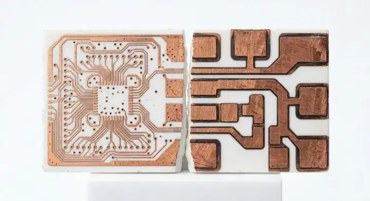
The core difference lies in the metallization method and resulting copper thickness: direct bonded copper (DBC) bonds thick copper foil (100–600µm) at ~1065°C for high-power applications, while direct plated copper (DPC) deposits thinner copper (10–150µm) via sputtering at ~300°C to achieve fine-pitch traces down to 50µm. Both technologies work with standard Al₂O₃ (Alumina) and high-conductivity AlN (Aluminum Nitride) base substrates.
Here is the breakdown of how these parameters compare side-by-side:
| Specification | DBC (Direct Bonded Copper) | DPC (Direct Plated Copper) |
|---|---|---|
| Bonding Temp | ~1065°C eutectic oxidation | ~300°C vacuum sputtering |
| Copper Thickness | 100µm – 600µm | 10µm – 150µm |
| Min Trace/Space | ~150µm (thick Cu limited) | 75µm (down to 50µm) |
| PTH Capability | No | Yes (laser drilled, Cu filled) |
| Surface Flatness | Rougher | Excellent (Ra < 0.3µm) |
| Bonding Strength | Extremely high mechanical bond | High chemical/sputtered bond |
Choose DBC if your design requires thick copper for continuous currents exceeding 100A; choose DPC if you need ultra-flat surfaces (Ra < 0.3µm) for LED die attach or fine-pitch RF routing.
Bottom line: Use DBC for heavy-duty brute-force power management, and default to DPC for high-precision, dense circuitry where trace geometry matters more than raw current capacity.
How Does the Manufacturing Process Differ Between DPC and DBC?
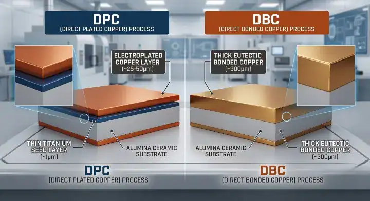
DBC manufacturing involves heating copper and ceramic to ~1065°C to create a eutectic Cu-O liquid melt that bonds the heavy foil directly to the substrate, whereas DPC uses a low-temperature ~300°C vacuum sputtering process to apply a thin titanium seed layer, followed by standard PCB electroplating to build the final copper thickness. These distinct chemical and physical approaches dictate the ultimate physical limitations of the boards.
Because DBC relies on pre-rolled copper foil bonded via extreme heat, the resulting surface is robust but structurally limited to simpler layouts. DPC, on the other hand, borrows techniques from the semiconductor industry.
The DPC process sequence involves:
- Cleaning the bare ceramic substrate in a vacuum chamber.
- Sputtering a thin adhesion layer (usually Titanium or Chromium).
- Sputtering a thin copper seed layer.
- Applying photoresist and exposing the circuit pattern.
- Electroplating copper up to the desired thickness (up to 150µm).
- Stripping the resist and etching away the ultra-thin seed layer.
Bottom line: The DBC process behaves like heavy mechanical welding, while the DPC process functions as highly controlled, semi-conductor-grade chemical deposition.
What Copper Thickness and Line Width Can Each Process Achieve?
DBC ceramic substrates achieve heavy copper thicknesses of 100µm to 600µm with minimum trace/space limits around 150µm, while DPC boards support thinner copper profiles of 10µm to 150µm but excel at ultra-fine minimum traces of 75µm (down to 50µm). Knowing how to evaluate a ceramic PCB manufacturer requires checking their specific etching tolerances for these parameters.
You can apply a strict current threshold decision rule to your design phase: below 30A use DPC, from 30A to 100A consider both based on trace density, and above 100A default to DBC.
| Power Level | Routing Requirement | Recommended Metallization |
|---|---|---|
| Low (<30A) | High density (<100µm traces) | DPC |
| Medium (30–100A) | Standard density (>150µm traces) | DPC or DBC |
| High (>100A) | Low density (power planes) | DBC |
Choose DPC for sub-100µm line widths in compact sensor modules; choose DBC when carrying massive amperages in electric vehicle powertrains where 300µm+ copper is mandatory.
Here is the catch: Thick copper inherently suffers from isotropic etching. If a supplier tries to etch a 150µm gap into 300µm thick DBC copper, the etchant will undercut the trace, creating a trapezoidal cross-section that ruins impedance and trace reliability.
Bottom line: If your layout requires traces finer than 150µm, DBC is structurally off the table due to heavy copper etching limitations.
Which Process Handles Thermal Cycling and Reliability Better?
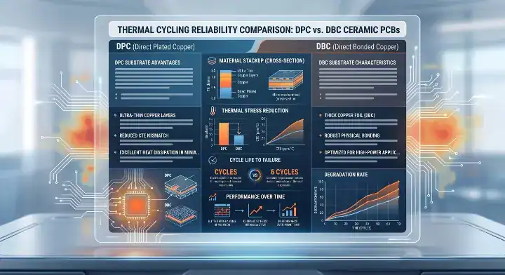
DPC generally survives thermal cycling better than DBC on standard Al₂O₃ because its thinner copper generates less physical thermal stress, whereas thick-copper DBC Al₂O₃ substrates show over a 50% failure rate from delamination after just 40 cycles from -55°C to +150°C. This is driven by severe CTE (Coefficient of Thermal Expansion) mismatch between the ceramic and the metal.
A common complaint on hardware forums reads: “Got ceramic boards, copper peeled after soldering, supplier claims soldering temp was too high, is it true?” The definitive answer is no. Standard reflow at 245°C cannot cause peeling on properly manufactured boards. Ceramic PCB copper peeling prevention dictates that peel strength must hit a minimum of 1.4 N/mm per IPC Class 3. If copper peels during assembly, it indicates a severe fabrication defect—such as bad eutectic bonding for DBC or a poor Ti seed layer for DPC—not an assembly temperature issue.
The mechanics of CTE mismatch solder joint failures are well documented. Research on Al₂O₃-DBC substrates found that over half of substrate failures occurred from delamination within 40 thermal cycles between -55°C and +150°C, with fatigue cracks initiating at copper pad edges and propagating into the ceramic at 15-30° angles. This occurs because Al₂O₃ has a CTE of 6.9 ppm/°C compared to copper’s 16.4 ppm/°C. DPC’s thinner copper simply exerts less pulling force on the ceramic during rapid temperature swings. To survive 5,000+ cycles, engineers must upgrade to Si₃N₄ (Silicon Nitride) substrates using AMB or advanced DBC techniques. Ensure you configure your ceramic PCB soldering reflow profile properly to avoid shocking components, even if the board itself is robust.
In our internal PCB production, we process thousands of these panels. The most common reliability failure isn’t from the end application—it’s from incoming material quality. About 12% of DBC substrates from secondary suppliers arrive with micro-voids at the copper-ceramic interface. These voids become crack initiation points after just a few reflow cycles, which is why we run 100% ultrasonic scanning on every incoming DBC batch. On the DPC side, the critical checkpoint is Ti seed layer uniformity; anything below 50nm thickness will delaminate under thermal stress due to poor chamber vacuum levels during sputtering.
Bottom line: A peeling trace during standard SMT reflow is a red flag for a factory defect; specify DPC for extreme thermal cycling environments unless you upgrade your DBC base to Silicon Nitride.
Can You Get Plated Through Holes on DBC or DPC Ceramic PCB?
DBC cannot support plated through holes (PTH) because its bonded foil process cannot plate inside ceramic cavities, whereas DPC fully supports laser-drilled, copper-filled vias to enable double-sided and multilayer designs. This is often the single most critical gating factor for complex schematics.
A recurring question across engineering platforms is: “Can DBC do plated through holes?” The answer is a hard no. Because DBC relies on oxidizing pre-cut copper foils at over 1000°C, there is no chemical mechanism to deposit copper onto the vertical sidewalls of a hole drilled through the ceramic.
Here is how DPC solves this:
- A laser drills precise vias through the bare ceramic before metallization.
- The vacuum sputtering process deposits the Ti/Cu seed layer over the surface and down through the via walls.
- The subsequent electroplating phase fills the via with solid copper.
- The result is a highly conductive, thermally efficient path between top and bottom layers.
Bottom line: If your design requires a via to connect signals or thermal planes between the top and bottom layers, you must use DPC metallization.
How Does DPC vs DBC Ceramic PCB Cost Compare?
At mid-volume production (100–500 boards), DPC boards typically cost $3 to $8 per unit, while standard DBC boards range from $5 to $12 per unit due to the energy-intensive high-temperature bonding process and thicker raw copper material costs. Pricing shifts based on the specific scenario and volume requirements.
| Volume Scenario | DPC Cost Estimate (Per Unit) | DBC Cost Estimate (Per Unit) | Turnaround Time |
|---|---|---|---|
| Prototype (5–10 pcs) | $40 – $90 (Lower NRE) | $60 – $130 (Higher NRE) | 2–3 weeks |
| Mid-Volume (100–500 pcs) | $3 – $8 | $5 – $12 | 3–4 weeks |
| Production (1,000+ pcs) | $1.50 – $4 | $3 – $8 | 4–6 weeks |
For prototype runs, expect DPC to provide a distinct cost advantage because sputtering requires less initial tooling; for high-volume automotive production, the slightly higher unit cost of DBC is easily justified by its massive current-handling capabilities.
Because NRE (Non-Recurring Engineering) fees for DBC involve custom tooling for copper foil stamping and high-temperature fixtures, initial setup costs run higher. DPC uses standard photo-lithography masks which are much cheaper to generate on short notice.
Bottom line: DPC offers superior cost-efficiency for prototyping and high-density, low-power applications, while DBC pricing scales heavily alongside required copper thickness.
When Should You Choose DBC Over DPC (and Vice Versa)?
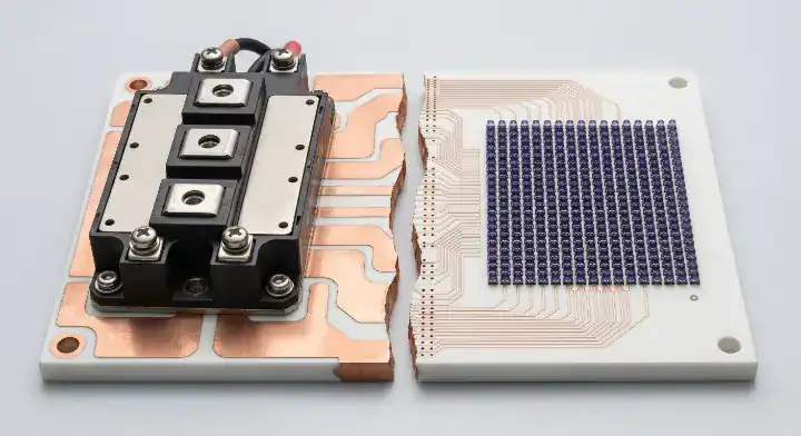
Choose a DBC ceramic substrate for high-power IGBT modules, motor drives, and EV inverters handling over 100A, while DPC is the superior choice for high-brightness LED modules, RF circuits, and semiconductor packaging requiring fine traces. Your choice should directly align with your most restrictive engineering constraint.
Here is the breakdown of ideal applications:
- Green flag for DBC: You are designing solar power converters or heavy traction inverters requiring 300µm+ copper planes to dissipate raw heat.
- Green flag for DPC: You are building compact optical transceivers, automotive LED headlights, or microwave RF boards requiring tight 75µm impedance control and perfectly flat pad surfaces.
Sometimes, a single technology isn’t enough. A European EV power module client came to us after their existing DBC supplier couldn’t achieve the 100µm trace/space needed for a redesigned gate driver section. Their power stage required 300µm copper for 80A continuous current. We engineered a hybrid approach: DBC Al₂O₃ for the power stage paired with a DPC AlN board for the gate driver section (35µm copper, 75µm trace). The DPC board gave them plated through holes to connect top-side gate signals to a bottom thermal pad. This reduced their module footprint by 22%, passed 2,000 thermal cycles (-40°C to +150°C) with zero delamination, and was prototyped in just 4 weeks.
If you need help reviewing your layout for these specific constraints, we offer a free DFM/DFA engineering review on every order to catch trace/space violations before fabrication.
Bottom line: Match the metallization to your hardest constraint—use DBC if amperage dictates the layout, and DPC if space, vias, and routing density are the bottlenecks.
How Do You Inspect and Qualify DPC vs DBC Boards from Your Supplier?
Qualifying these boards requires checking DBC for eutectic bonding voids using ultrasonic scanning, while DPC boards must be inspected for titanium seed layer uniformity and surface flatness (Ra < 0.3µm) using SEM cross-sections. Visual inspection alone is entirely inadequate for high-reliability ceramic substrates.
IPC standards establish a minimum acceptable peel strength of 1.4 N/mm (approximately 8 lb/in) for high-reliability Class 3 ceramic substrates, with testing per IPC-TM-650 method 2.4.8 (90° peel test). Your incoming quality control (IQC) team must request specific documentation.
| Inspection Item | DBC Boards | DPC Boards |
|---|---|---|
| Bonding Interface | Ultrasonic Scan (SAM) for voids | SEM cross-section for Ti layer |
| Adhesion Test | 90° Peel Test (>1.4 N/mm) | 90° Peel Test (>1.4 N/mm) |
| Trace Geometry | Check for severe undercut | AOI for shorts/opens |
| Surface Finish | Check for oxidation | Surface Profilometer (Ra < 0.3µm) |
Reject a DBC batch if ultrasonic scanning reveals micro-voids larger than 5% of the total pad area; reject a DPC batch if 90° peel tests drop below the mandatory 1.4 N/mm threshold.
Bottom line: Never rely on visual inspection to qualify ceramic PCBs; micro-voids in DBC and defective seed layers in DPC only reveal themselves under mechanical stress or acoustic imaging.
Conclusion
Understanding the precise limits of DPC vs DBC ceramic PCB technology prevents catastrophic thermal failures and routing dead-ends in your high-power designs. Relying on thick DBC copper for fine-pitch routing will cause undercutting, while using DPC for 150A power planes will literally melt the traces.
At QueenEMS, we bypass the guesswork. We offer full turnkey service—from component sourcing to final SMT/THT mixed assembly—with a 99.7% first-pass yield rate. We maintain up to 60-layer PCB fabrication capabilities and offer 3D AOI and X-Ray inspection on every BGA joint.
Stop wrestling with delamination and layout limitations. Partner with an EMS provider who understands the physics behind the board. Contact us today to get a free DFM review on your next ceramic PCB project.
Written by the QueenEMS Engineering Team
Frequently Asked Questions
Can I solder DPC ceramic PCB with standard SMT reflow? Yes. A standard reflow profile peaking at 245°C works perfectly for DPC boards. Because DPC utilizes a chemically sputtered titanium seed layer and electroplated copper, it easily withstands standard lead-free assembly temperatures without the copper peeling or bubbling.
Is DPC replacing DBC in all ceramic PCB applications? No. DBC remains strictly mandatory for ultra-high current applications handling over 100A. While DPC is dominating the high-density LED and RF markets due to its fine trace capabilities, it cannot deposit the massive 300µm+ copper thicknesses required for heavy industrial motor drives and EV traction inverters.
What is the minimum order quantity for DPC and DBC ceramic PCB? None. We support prototype runs as low as 5 units for both DPC and DBC technologies. Prototyping DPC is generally faster and cheaper due to lower tooling costs, while DBC prototypes require heavier initial setup but transition seamlessly into high-volume automotive production.
Can DBC ceramic PCB support plated through holes? No. The DBC process uses a solid bonded copper foil and extreme heat, meaning it cannot deposit conductive material inside a drilled ceramic hole. If your design mandates vias to connect top and bottom layers, you must switch to DPC metallization.
Upload your files today · Free DFM check before production · Ship worldwide
Get your PCB prototypes in as fast as 24 hours. We handle FR4, Rogers, and Flex up to 60 layers — free prototypes for 2–4 layer boards, no minimum order.
Just upload your Gerber + BOM — we source every part, assemble, and inspect (AOI + X‑Ray) so you don't have to chase suppliers. Boards ship in as fast as 24 hours.