
Quick Answer: The decision between a thick film vs thin film ceramic PCB comes down to line width and operating frequency. You should choose thick film for power electronics operating under 1 GHz with trace widths ≥ 75 μm to save 40–60% on costs. You must upgrade to thin film (or DPC) when your design operates above 2 GHz or requires high-density sub-50 μm trace widths, as thin film delivers an ultra-smooth surface (Ra < 0.5 μm) that eliminates RF skin effect losses.
Key takeaways:
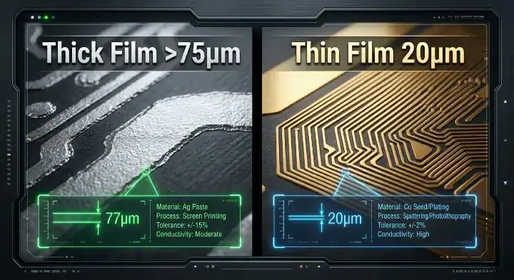
- Thick film prints conductive paste at 10–25 μm thickness, while thin film sputters copper at < 1 μm.
- Thin film achieves dense 5–20 μm trace widths; standard thick film safely stops at 75 μm.
- Thick film allows you to embed resistors and capacitors directly into the board during firing.
- Thin film reduces insertion loss by 30–50% at 5 GHz compared to thick film due to lower surface roughness.
Table of Contents
- What Is the Core Difference Between Thick Film and Thin Film Ceramic PCB?
- How Are Thick Film and Thin Film Ceramic PCBs Made?
- What Are the Line Width and Precision Limits of Each Process?
- Which Process Handles High-Frequency RF Applications Better?
- How Do Costs Compare Between Thick Film and Thin Film Ceramic PCBs?
- Which Process Should You Choose for Power Electronics?
- Can You Embed Passive Components Into Thick Film Ceramic PCBs?
- What Are the Most Frequently Asked Questions About Ceramic Processes?
Are you overpaying for ceramic manufacturing precision you don’t actually need, or are you losing high-frequency signals because your substrate is too rough? Misunderstanding the boundary between ceramic processing technologies destroys project budgets and ruins signal integrity. Getting this choice right matters; at QueenEMS, our production data shows a 99.7% first-pass yield rate when clients perfectly match their trace requirements to the correct ceramic manufacturing method.
What Is the Core Difference Between Thick Film and Thin Film Ceramic PCB?
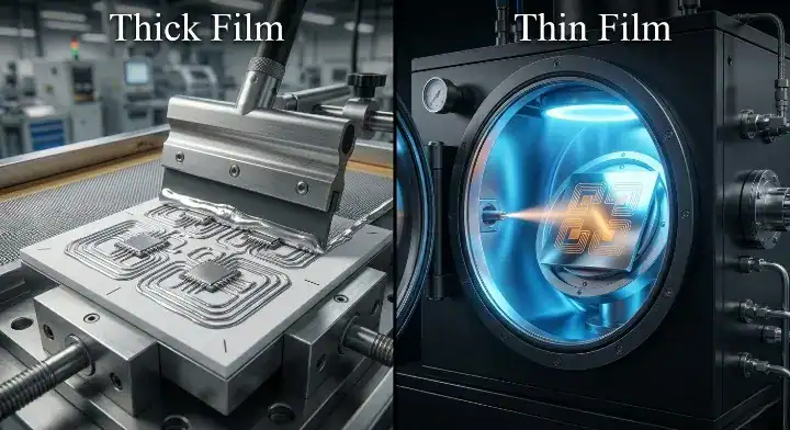
The core difference between a thick film vs thin film ceramic PCB is how the conductive metal bonds to the substrate. Thick film uses a screen-printing process to push a silver-palladium paste through a mesh, resulting in a 10–25 μm thick conductor layer, while thin film uses a vacuum sputtering chamber to deposit a microscopic copper layer typically < 1 μm thick. This physical difference dictates their applications: thick film dominates high-power automotive sensors, while thin film rules high-frequency telecom modules.
What about the middle ground? Many engineers get confused when they need a conductor thickness between 1 μm and 10 μm. This middle zone is neither thick nor thin film; it is DPC (Direct Plated Copper), where a thin sputtered seed layer is electroplated up to 10 μm or more. Reviewing our core ceramic PCB manufacturing capabilities clarifies exactly where DPC fits into your design matrix.
- Thick Film: 10–25 μm conductor thickness, printed via screen mesh.
- Thin Film: < 1 μm conductor thickness, sputtered in a vacuum.
- DPC (Direct Plated Copper): 1–10+ μm, combining sputtering and electroplating.
| Feature | Thick Film | Thin Film | DPC (Direct Plated Copper) |
|---|---|---|---|
| Conductor Thickness | 10–25 μm | < 1 μm | 1–10+ μm |
| Deposition Method | Screen printing | Vacuum sputtering | Sputtering + Plating |
| Typical Line Width | ≥ 75 μm | 5–20 μm | 30–50 μm |
Choose thick film if you need rugged, low-cost current carrying capacity. Choose thin film or DPC if you are routing highly dense sub-50 μm traces.
Bottom line: Base your initial technology decision strictly on how the metal is applied: print thick film for power, or sputter thin film for precision.
How Are Thick Film and Thin Film Ceramic PCBs Made?
To build a thick film ceramic PCB, a factory screen-prints conductive, resistive, or dielectric pastes onto an Al₂O₃ substrate and fires it at 850–900°C. To build a thin film ceramic PCB, the factory places the substrate in a vacuum chamber, uses physical vapor deposition (PVD) to lay down a titanium adhesion layer followed by copper, and then uses photolithography to etch highly precise patterns.
Can you mix them? Yes, a hybrid approach exists. For designs requiring both high power and high frequency, factories can print thick film power traces on one section of the board, and deposit thin film signal traces on another. Taking advantage of a free DFM review helps you determine if a hybrid approach is cost-effective for your specific layout.
- Thick film requires a simple screen printer and a high-temperature conveyor furnace.
- Thin film requires expensive vacuum chambers, PVD targets, and cleanroom photolithography.
- Both processes commonly use 96% or 99% alumina (Al₂O₃) or aluminum nitride (AlN) substrates.
Bottom line: The thin film manufacturing process is significantly more complex and requires cleanroom conditions, which directly drives up the unit cost compared to thick film.
What Are the Line Width and Precision Limits of Each Process?
When specifying a thick film ceramic PCB, the standard minimum line width is 75–100 μm, whereas a thin film ceramic PCB easily achieves ultra-dense 5–20 μm line widths due to its photolithographic etching. The IPC-7711/7721 standard mandates that thin film conductor layer thickness variations stay strictly within ±15%, a level of precision that screen-printed thick film paste physically cannot match.
Engineers on the EEVBlog forum frequently ask: “My design has a 50 μm line width requirement. A factory quoted me for thick film but didn’t state their minimums. Can thick film actually do 50 μm reliably?” The reality is yield loss. Standard thick film on 96% alumina safely stops at 75 μm. While a premium thick film line might occasionally print a 50 μm trace, the yield drops significantly. The correct approach is to demand the factory’s Process Capability (Cpk) data. If your design requires 50 μm traces, thin film handles this as a routine capability with a Cpk ≥ 1.33, making it the only safe choice for mass production.
- Thick Film minimum trace width: 75–100 μm (safe production).
- Thin Film minimum trace width: 5–20 μm (safe production).
- DPC minimum trace width: 30–50 μm (safe production).
Bottom line: If your layout features critical trace widths below 50 μm, you must abandon thick film and transition immediately to thin film or DPC technology.
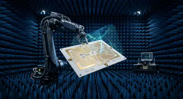
Which Process Handles High-Frequency RF Applications Better?
A thin film ceramic PCB dominates high-frequency RF applications because its ultra-smooth surface (Ra < 0.5 μm) and pure copper conductors reduce insertion loss by 30% to 50% at 5 GHz compared to standard thick film. According to IEEE Spectrum (spectrum.ieee.org), every 1 μm increase in surface roughness increases conductor loss by 15–20% at 10 GHz due to the skin effect, making thick film a poor choice for microwave frequencies.
Users on Electronics StackExchange often debate: “My design operates at 5.8 GHz. A factory claims thick film works for RF, but I’m worried about loss. Which process is actually better?” We have a definitive case study for this. A telecom client came to us with a 5.8 GHz transceiver module built on a thick film Al₂O₃ board. Their first batch showed a massive 3.2 dB insertion loss at 5.8 GHz. After cross-section analysis, we identified that the thick film silver conductor’s roughness (Ra ~2.1 μm) was causing excessive skin effect losses. We migrated their design to DPC thin film on 99.6% Al₂O₃, achieving an Ra < 0.4 μm. The second batch measured just 1.4 dB insertion loss—a 56% improvement. Navigating RF PCB requirements means acknowledging that physics strictly limits thick film at higher frequencies.
- Thick Film: Ra 1–3 μm (Too rough for frequencies above 2 GHz).
- Thin Film: Ra < 0.5 μm (Ideal for 5G, radar, and microwave).
- Conductor Material: Thin film pure copper conducts better than fired thick film silver-paste.
| Application Frequency | Recommended Process | Primary Limiting Factor |
|---|---|---|
| Sub-1 GHz | Thick Film | None (Highly cost-effective) |
| 1 GHz to 2 GHz | Thick Film or DPC | Trace width and routing density |
| 2 GHz to 10+ GHz | Thin Film | Surface roughness (Skin effect loss) |
Choose thin film immediately if your design operates above 2 GHz. Avoid thick film for RF unless your frequency is low and you are highly sensitive to unit cost.
Bottom line: High-frequency RF signals travel on the outer skin of the conductor; thin film provides the microscopic smoothness required to prevent these signals from scattering.
How Do Costs Compare Between Thick Film and Thin Film Ceramic PCBs?
At volume production, a thin film ceramic PCB typically costs 40% to 200% more than an equivalent thick film ceramic PCB because the vacuum sputtering equipment and cleanroom photolithography are vastly more expensive to operate than a conveyor belt screen printer. Furthermore, the NRE (Non-Recurring Engineering) cost for thin film requires expensive quartz or glass photomasks, making prototype runs 2 to 4 times more expensive than thick film setups.
Consider the scale: If you are building 10,000 basic automotive sensor boards, the high NRE and unit cost of thin film will destroy your margin.
- Prototype (5–10 pcs): Thin film NRE costs $500–$1,200; thick film NRE costs $150–$300.
- Mid-volume (100–500 pcs): Thin film adds $10–$25 per board over thick film.
- High-volume (1,000+ pcs): The 40–60% thin film premium remains due to slow vacuum cycle times.
Bottom line: Never specify thin film unless your density or frequency requirements absolutely demand it; thick film is always the better financial decision for standard layouts.
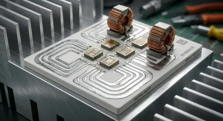
Which Process Should You Choose for Power Electronics?
For high-current power electronics, you should almost exclusively choose a thick film ceramic PCB because it effortlessly handles trace widths above 75 μm, provides excellent thermal dissipation, and costs significantly less than thin film. Power electronics prioritize heat spreading and high current capacity, making the microscopic precision of thin film entirely unnecessary.
In our production line, we see engineers struggle with the thick film vs thin film decision constantly when designing LED driver modules or automotive sensors. Here is where they fail: They specify thin film because they’ve heard it is “more precise.” But for a 200W LED driver featuring massive 2mm trace widths and zero RF components, thin film adds 60–80% to their substrate cost with absolutely zero performance benefit. We have redirected dozens of these projects back to thick film with AlN substrates. The thermal conductivity remains at 150–170 W/m·K, the copper easily carries the current, and the client saves $8–15 per substrate at 500-unit volumes. Applying correct ceramic PCB design rules prevents you from over-specifying your substrate.
- Red flag: Using thin film for traces wider than 100 μm.
- Green flag: Using thick film for high-power LED arrays and motor drives.
- Decision Rule: Trace > 75 μm + Freq < 1 GHz = Always Thick Film.
| Design Requirement | Trace Width | Operating Frequency | Decision |
|---|---|---|---|
| High-power LED Driver | > 1.0 mm | DC / Low Hz | Thick Film |
| 5G Antenna Module | < 50 μm | 5.8 GHz | Thin Film |
| Automotive Sensor | > 100 μm | Sub-1 GHz | Thick Film |
Choose thick film for heavy power routing where heat dissipation is the only major concern. Choose thin film only when power routing is mixed with dense, high-frequency logic.
Bottom line: If your power electronics design does not require sub-50 μm traces or GHz frequencies, thin film is an expensive mistake; thick film will perform identically for less money.
Can You Embed Passive Components Into Thick Film Ceramic PCBs?
Yes, a major advantage of a thick film ceramic PCB is the ability to embed passive components directly into the board by screen-printing resistive and dielectric pastes and co-firing them with the conductors. Thin film processes completely lack this ability, meaning all resistors and capacitors on a thin film board must be externally sourced and soldered to the surface.
Why does embedded tech matter? By printing thick film resistors directly onto the alumina substrate, you eliminate SMT solder joints, drastically reducing your BOM count and improving vibration reliability. This is heavily utilized in high-frequency PCB assembly where space is at an absolute premium.
- Thick film embeds resistors via Ruthenium oxide paste.
- Thick film embeds capacitors via Barium titanate dielectric paste.
- Thin film requires surface-mounted (SMD) passive components.
Bottom line: If your design requires burying dozens of passive resistors to save board space or increase vibration resistance, thick film is your only viable ceramic option.
What Are the Most Frequently Asked Questions About Ceramic Processes?
What is the minimum line width for thick film ceramic PCB? Standard thick film ceramic PCB achieves a minimum line width of 75–100 μm on 96% alumina substrates. Premium thick film processes can reach 50 μm but with severely reduced manufacturing yield. If your design requires line widths below 50 μm, you must switch to thin film or DPC ceramic PCB.
Is thin film ceramic PCB always better than thick film? No. Thin film is only better for RF/microwave applications above 2 GHz and dense designs requiring sub-50 μm traces. For power electronics, LED drivers, and standard sensors with trace widths above 75 μm operating below 1 GHz, thick film ceramic PCB delivers the exact same thermal performance at 40–60% lower substrate cost.
Can thick film ceramic PCB embed resistors and capacitors? Yes. Thick film technology allows resistive and dielectric pastes to be screen-printed and co-fired directly on the ceramic substrate, successfully embedding resistors and capacitors into the board. This is one of thick film’s major advantages over thin film, which cannot integrate passive components during its manufacturing cycle.
Choosing between thick and thin film determines whether your project hits its budget or fails its RF testing. We know that balancing high-frequency performance against prototype costs is a difficult engineering challenge. At QueenEMS, we run both thick film and DPC/thin film lines, allowing us to guide you to the exact process your design requires without bias. If you are unsure which technology fits your next module, contact us to review your layout and trace density requirements today.
Written by the QueenEMS Engineering Team
Upload your files today · Free DFM check before production · Ship worldwide
Get your PCB prototypes in as fast as 24 hours. We handle FR4, Rogers, and Flex up to 60 layers — free prototypes for 2–4 layer boards, no minimum order.
Just upload your Gerber + BOM — we source every part, assemble, and inspect (AOI + X‑Ray) so you don't have to chase suppliers. Boards ship in as fast as 24 hours.